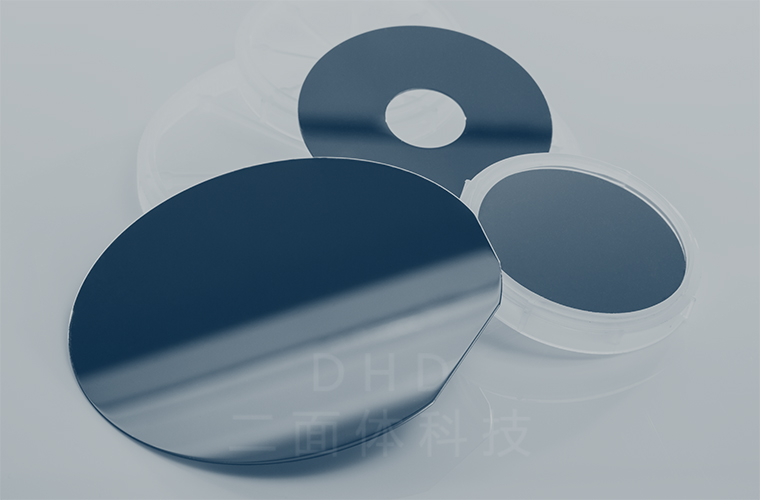
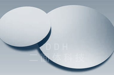
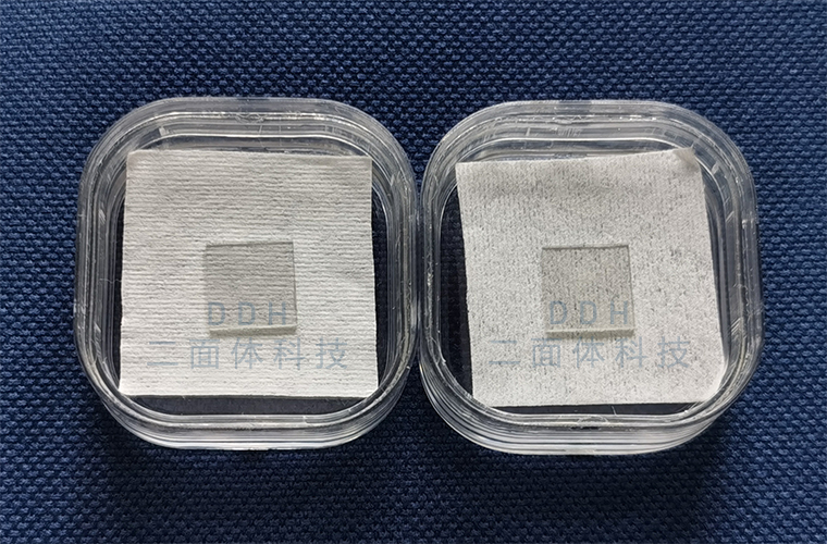
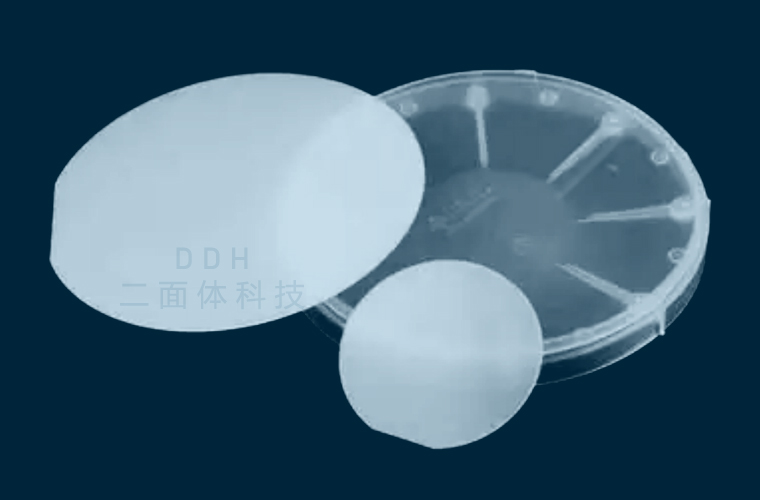
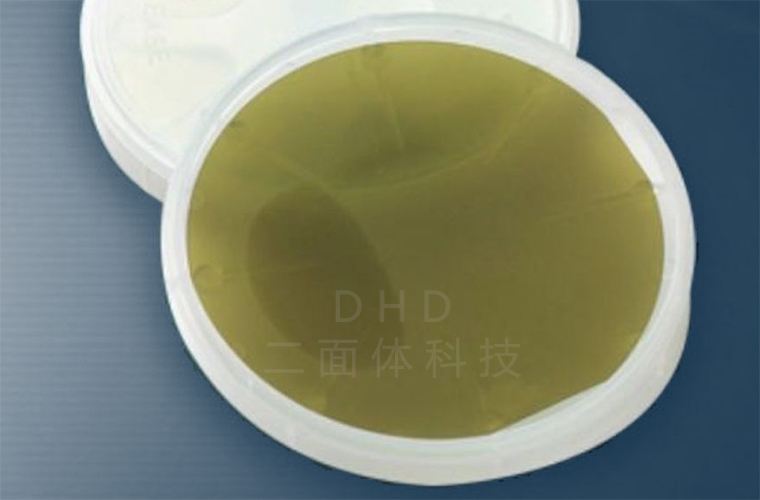
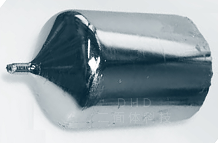
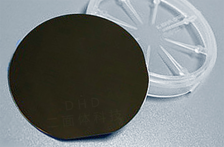
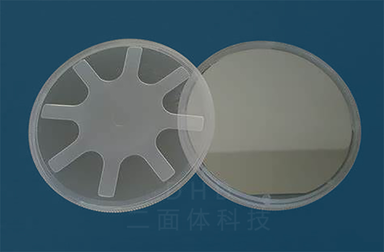
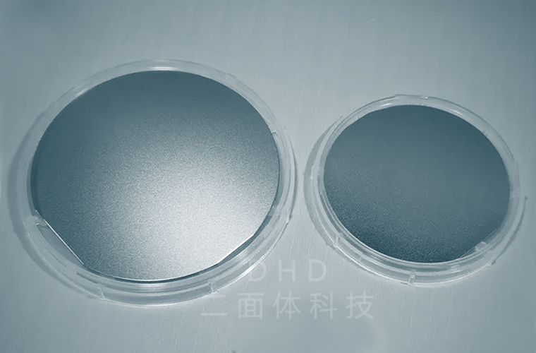
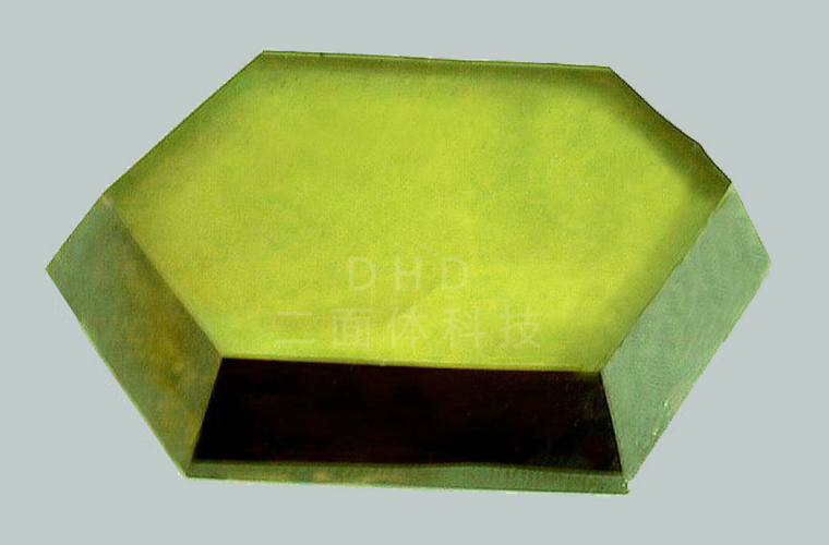
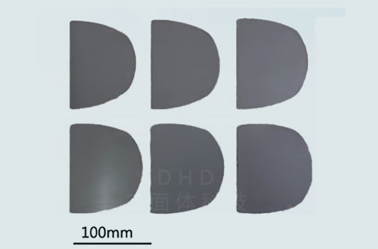
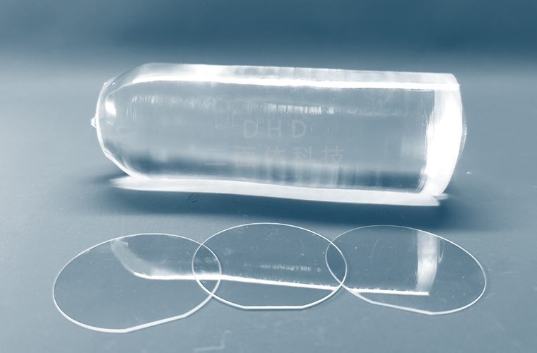
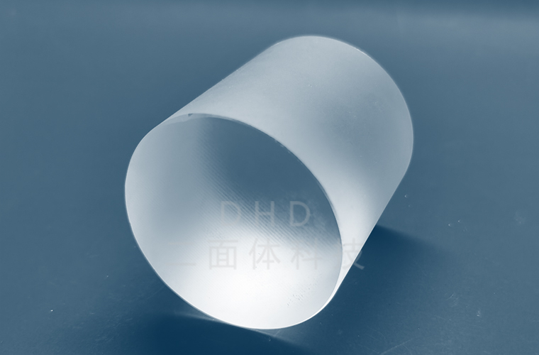
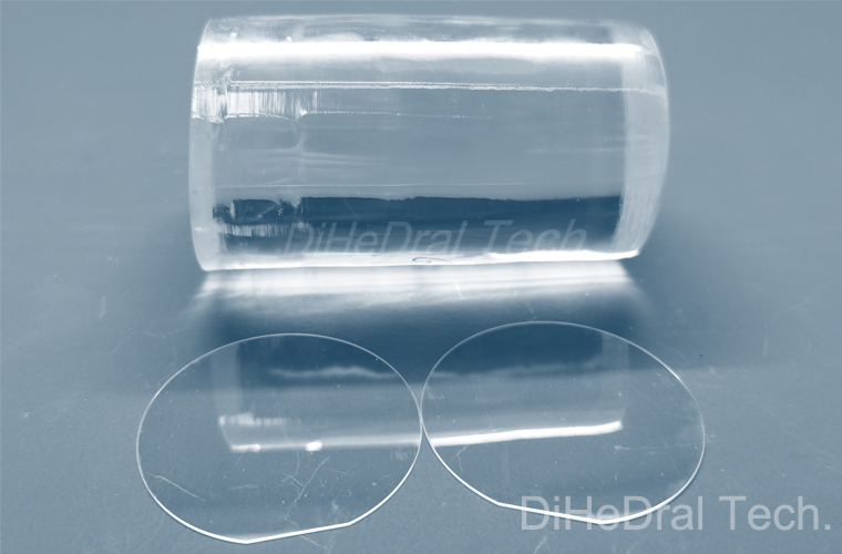
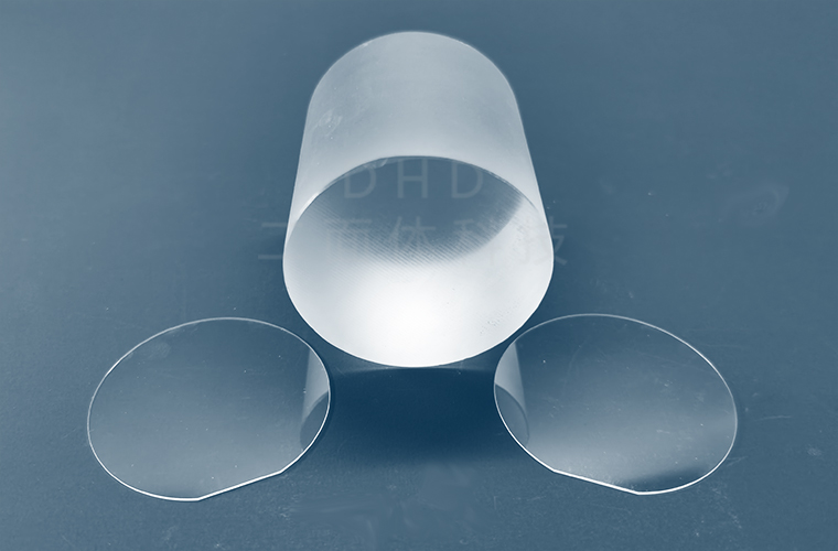
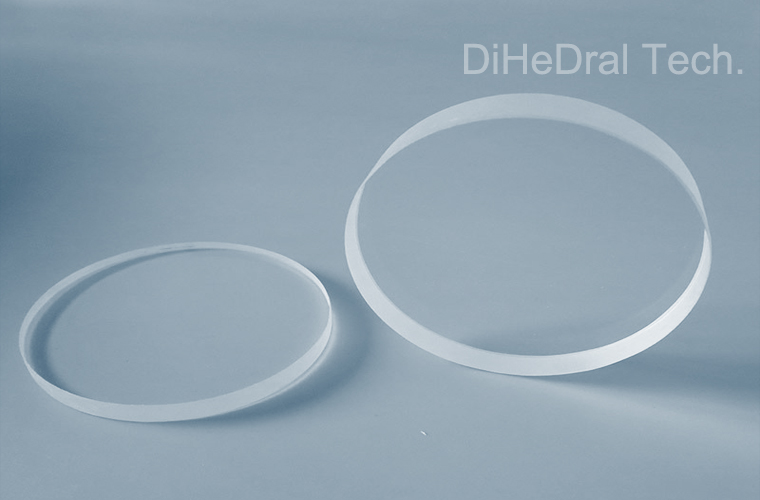
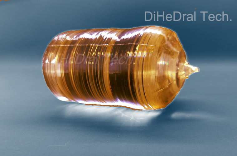
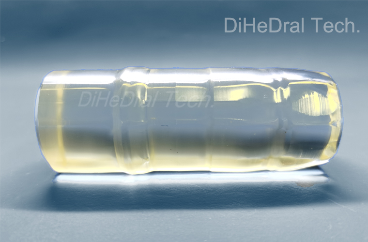
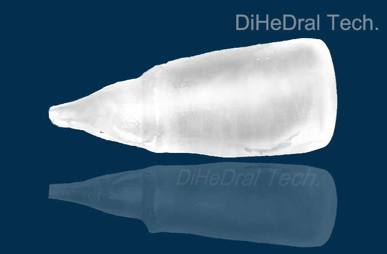
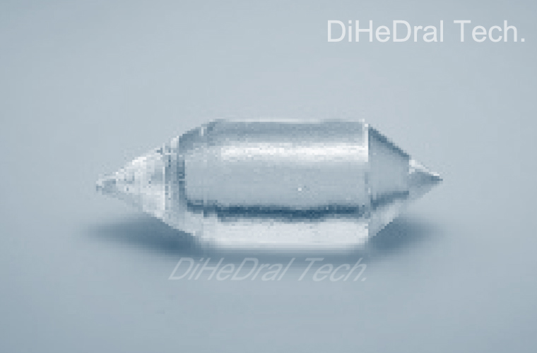
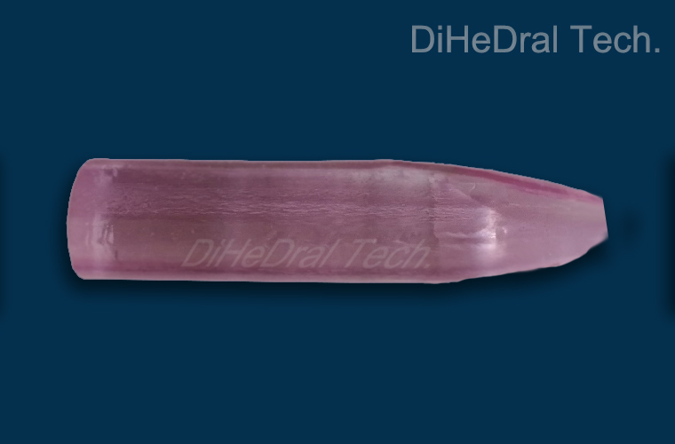
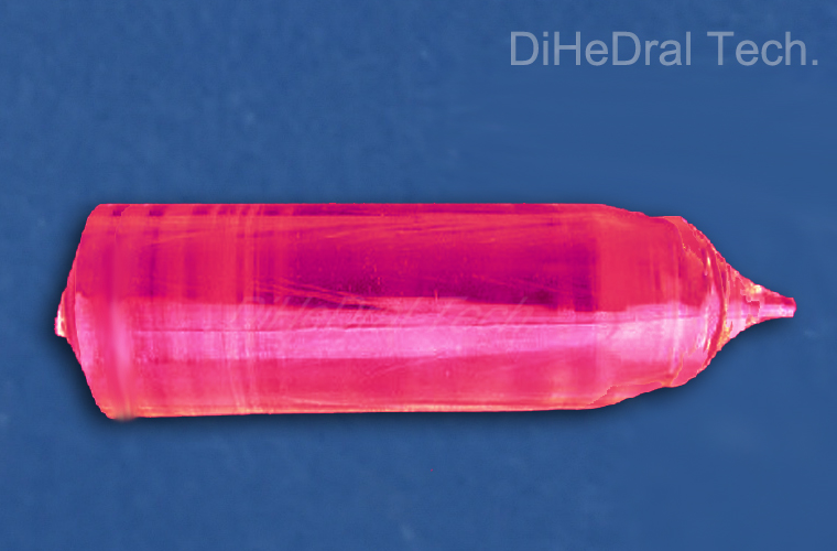
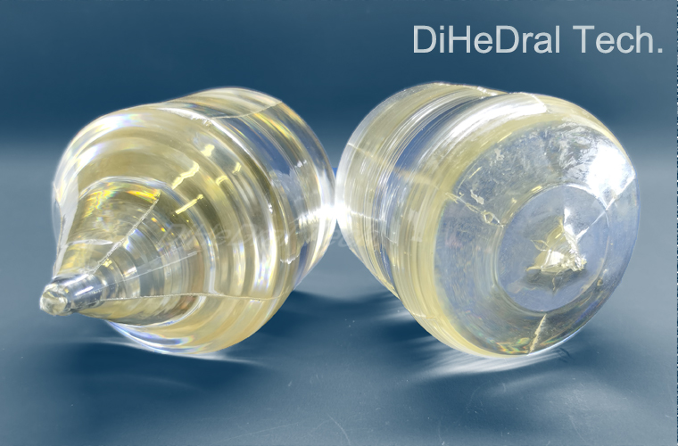
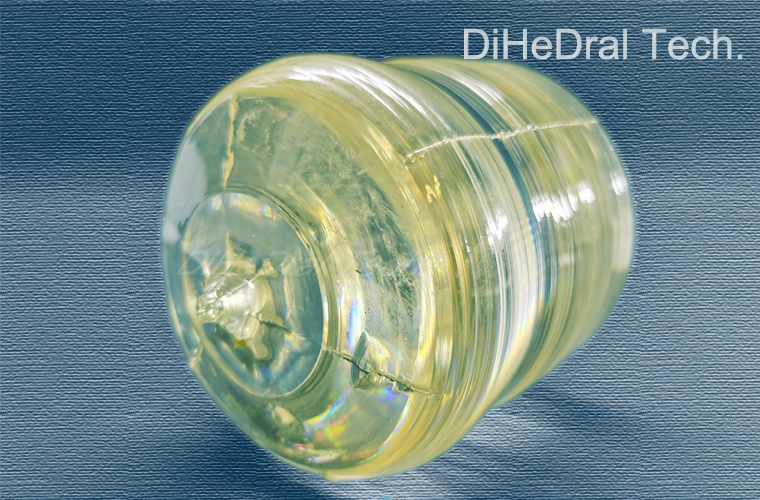
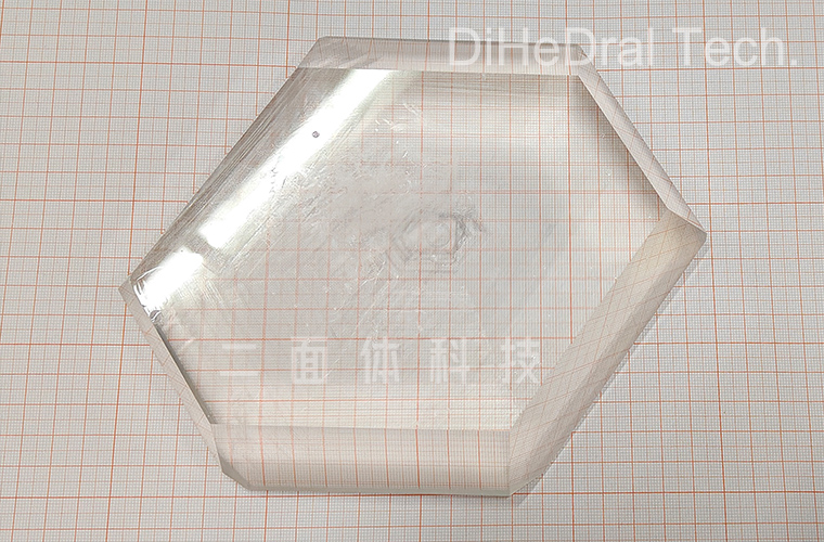
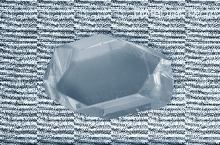
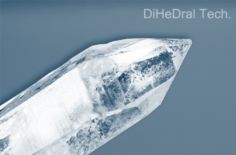
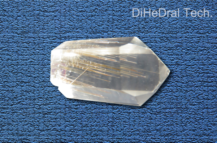
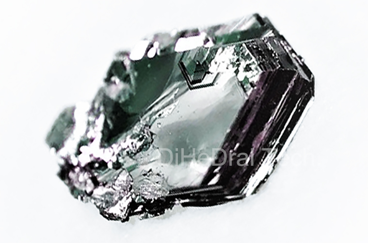
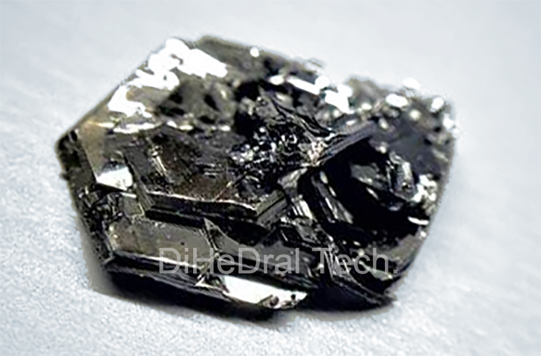
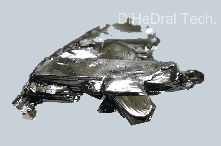
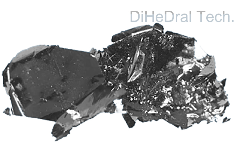
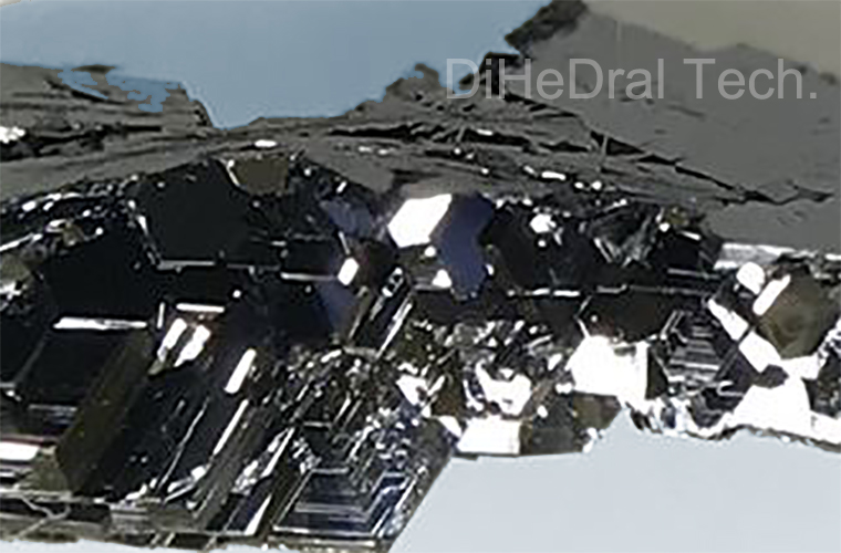
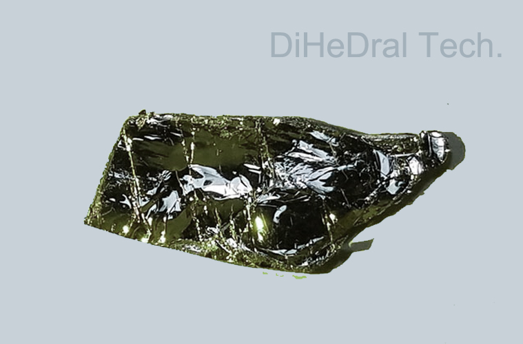
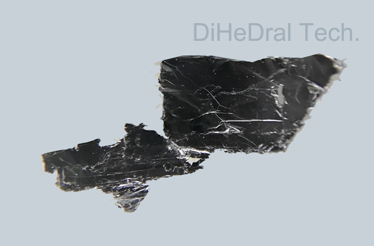
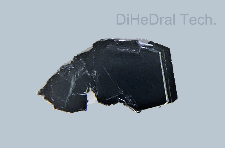
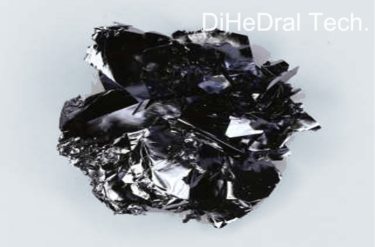
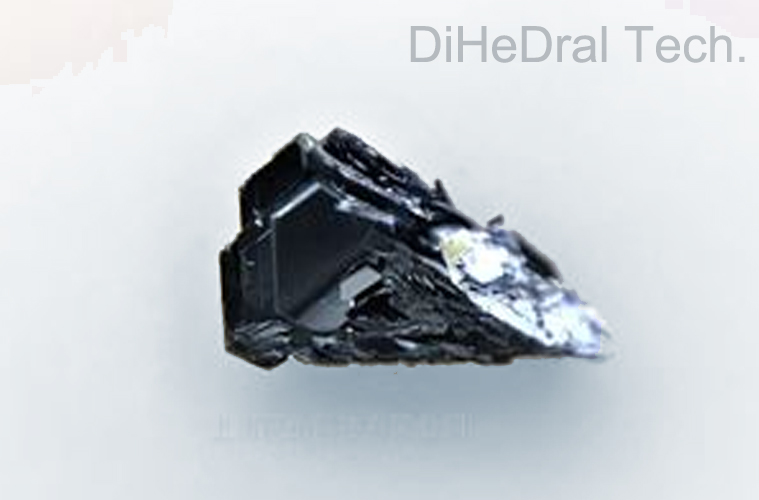
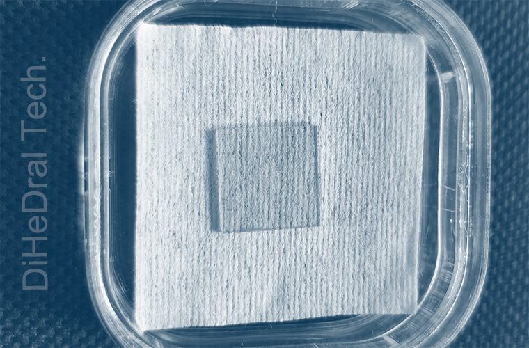
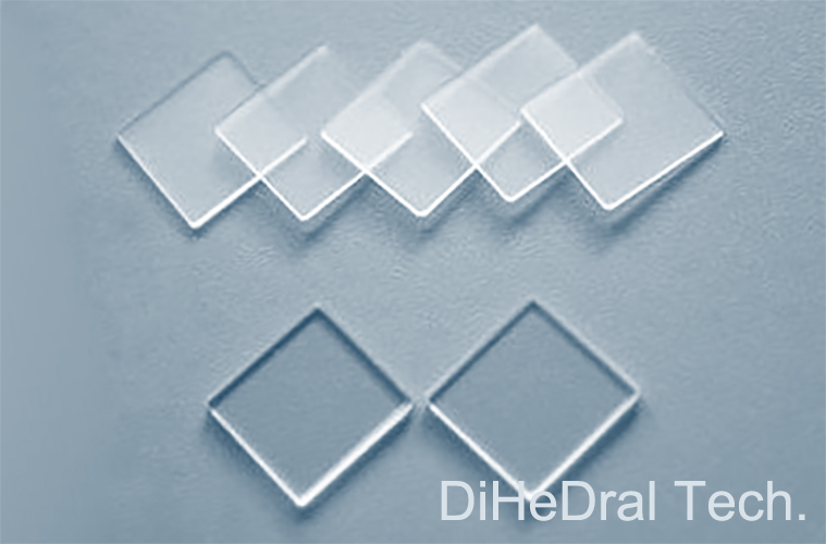
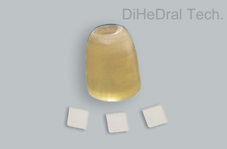
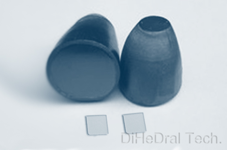
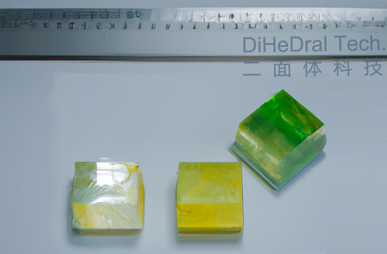
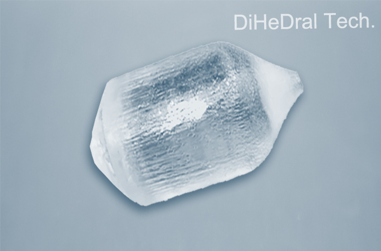
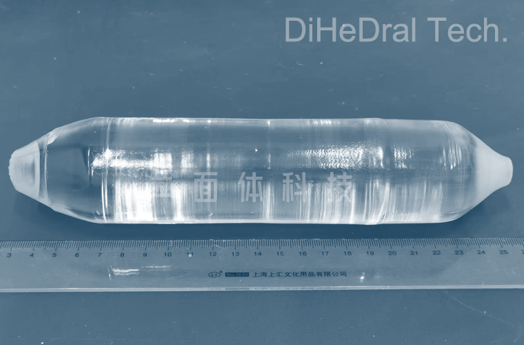
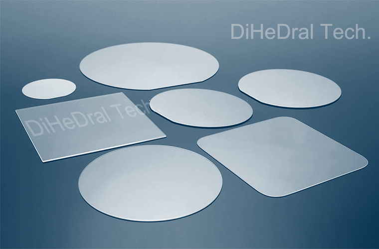
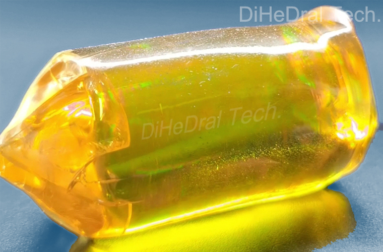
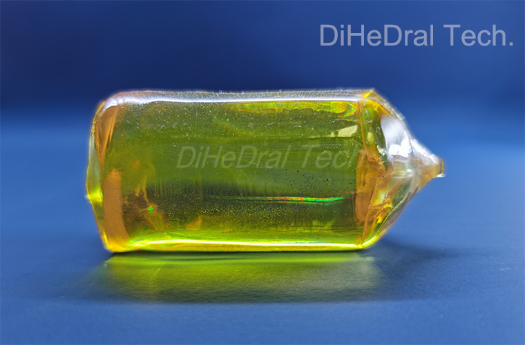
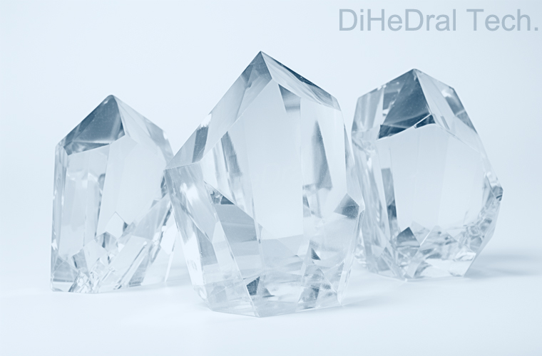
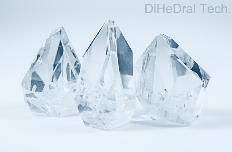
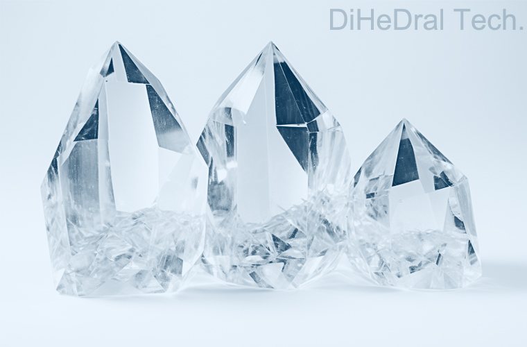
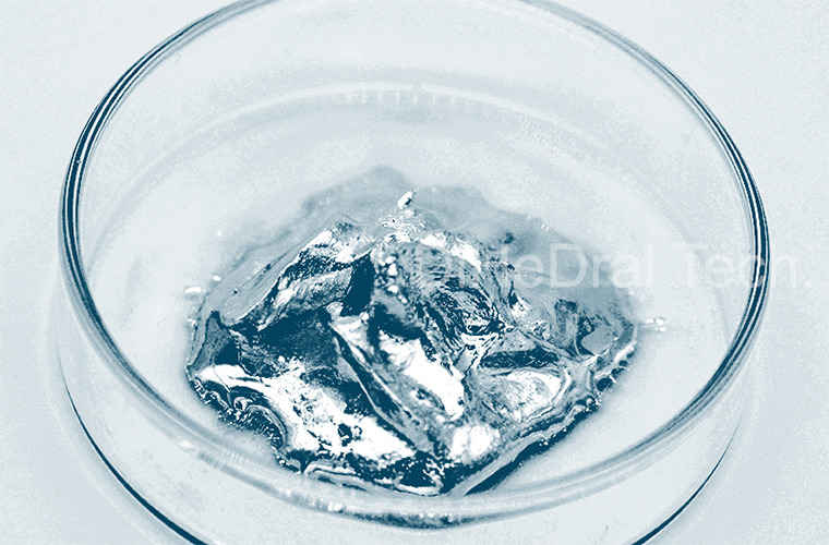
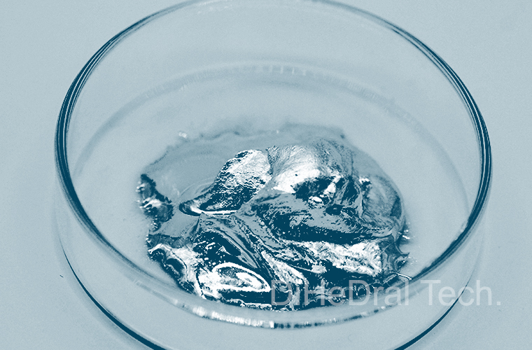
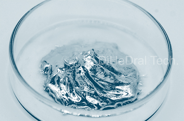
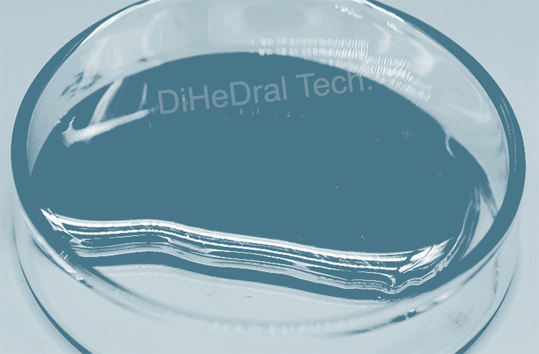
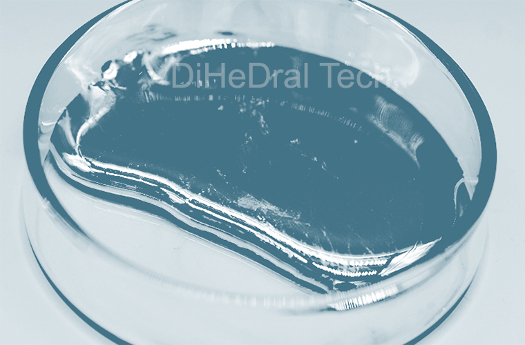
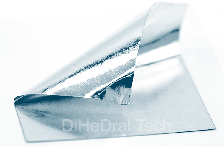
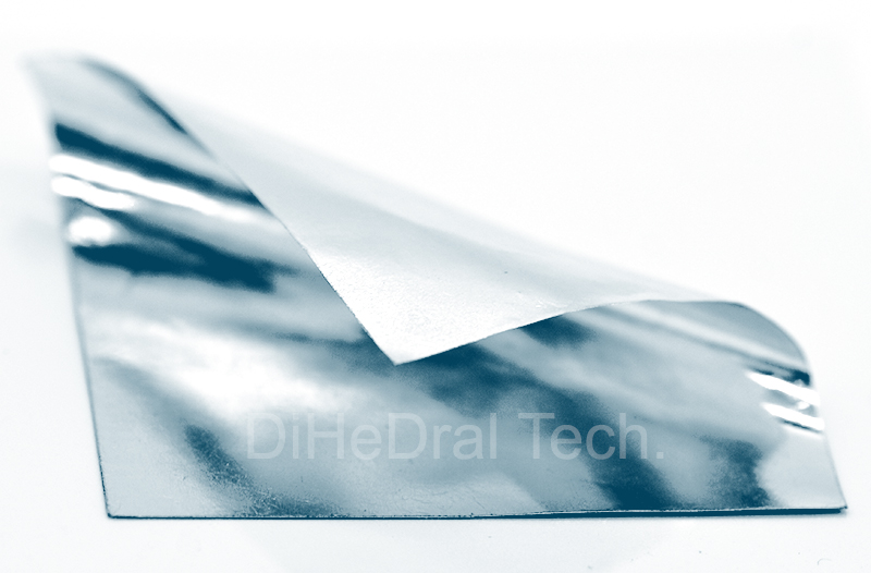
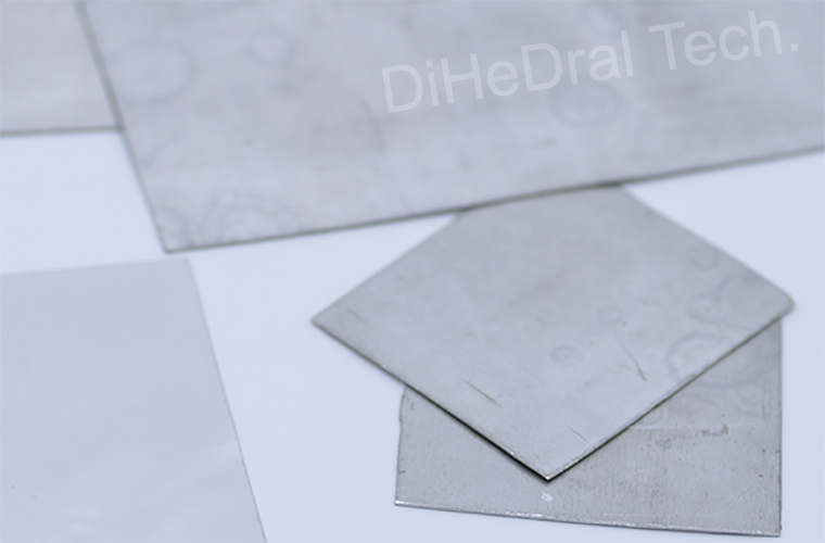
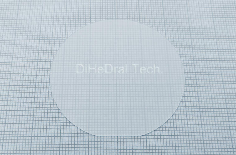
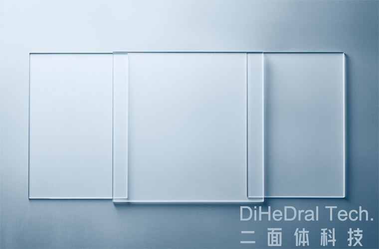
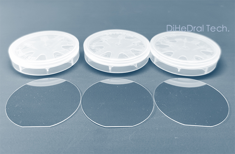
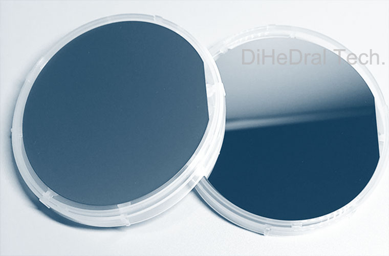
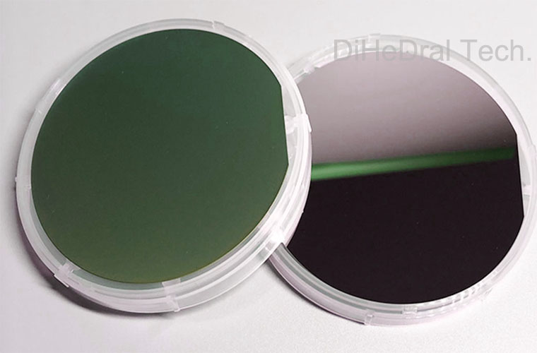
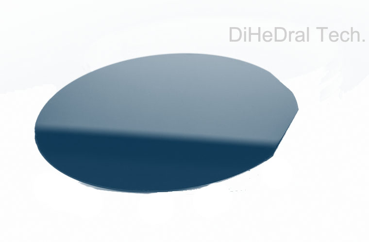
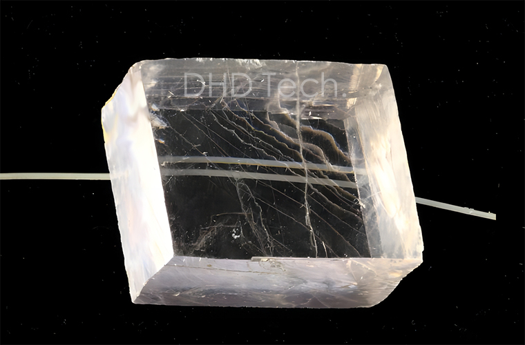
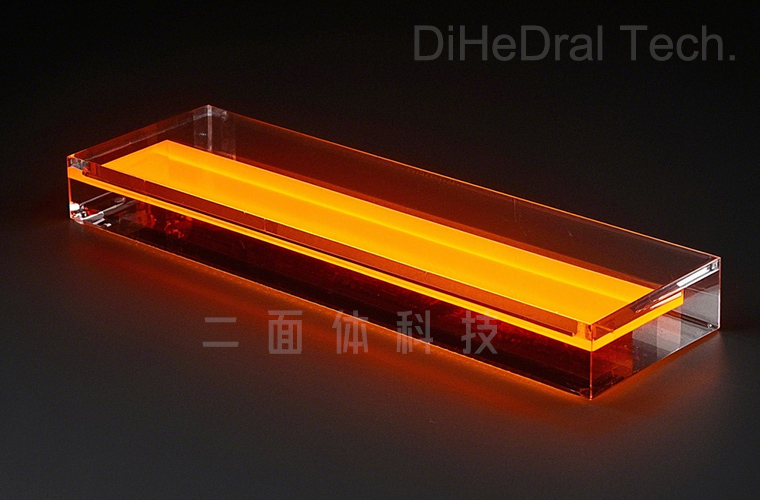
Links
N S A A
Dihedral (Shanghai) Science and Technology Co., Ltd Logo Dihedral (Shanghai) Science and Technology Co., Ltd
  • Home
  • Products
      • Semiconductor crystal
        • Elemental semiconductor
          • Diamond (C)
          • Silicon (Si)
          • Germanium (Ge)
        • Compound semiconductor
          • Gallium oxide (Ga2O3)
          • Gallium nitride (GaN)
          • Silicon carbide (SiC)
          • Gallium arsenide (GaAs)
          • Indium phosphide (InP)
          • Gallium antimonide (GaSb)
          • Indium arsenide (InAs)
          • Zinc oxide (ZnO)
          • Cadmium zinc telluride (CdZnTe)
          • Aluminum Nitride (AlN) crystal/substrate/film
      • Single crystal substrate
        • Multifunctional single crystal substrate
          • Barium titanate (BaTiO3)
          • Strontium titanate (SrTiO3)
          • Iron doped strontium titanate (Fe:SrTiO3)
          • Neodymium doped strontium titanate (Nd:SrTiO3)
          • Aluminium oxide (Al2O3)
          • Potassium tantalum oxide (KTaO3)
          • Lead magnesium niobate–lead titanate (PMN-PT)
          • Magnesium oxide (MgO)
          • Magnesium aluminate spinel (MgAl2O4)
          • Lithium aluminate (LiAlO2)
          • Lanthanu m aluminate (LaAlO3)
          • Lanthanu m strontium aluminate (LaSrAlO4)
          • (La,Sr)(Al,Ta)O3
          • Neodymium gallate (NdGaO3)
          • Terbium gallium garnet (TGG)
          • Gadolinium gallium garnet (GGG)
          • Sodium chloride (NaCl)
          • Potassium bromide (KBr)
          • Potassium chloride (KCl)
      • Functional crystal
        • Optical window
          • Magnesium fluoride (MgF2)
          • Calcium fluoride (CaF2)
          • Barium fluoride (BaF2)
          • Lithium fluoride (LiF)
          • Yttrium aluminium garnet (YAG)
        • Scintillation crystal
          • Cerium doped lutetium yttrium orthosilicate (Ce:LYSO)
          • Cerium doped yttrium aluminium garnet (Ce:YAG)
          • Cerium doped yttrium aluminium perovskite (Ce:YAP)
          • Bismuth germanate (BGO)
          • Cadmium tungstate (CdWO4)
          • Ce:CLLB crystal
        • Laser crystal
          • Rare earth doped lithium yttrium fluoride (RE:LiYF4)
          • Rare earth doped lithium lutetium fluoride (RE:LiLuF4)
          • Ytterbium doped yttrium aluminium garnet (Yb:YAG)
          • Neodymium doped yttrium aluminium garnet (Nd:YAG)
          • Erbium doped yttrium aluminium garnet (Er:YAG)
          • Holmium doped yttrium aluminium garnet (Ho:YAG)
          • Nd,Yb,Er,Tm,Ho,Cr,Lu Infrared laser crystal
        • N* crystal
          • Lithium niobate (LiNbO3)
          • Lithium tantalate (LiTaO3)
          • Potassium hydrogen phthalate (KAP)
          • Potassium titanyl phosphate (KTP)
          • Quartz (SiO2)
          • Titanium dioxide (TiO2)
          • Tellurium dioxide (TeO2)
          • Yttrium aluminate (YAlO3)
          • Iceland Spar
        • Metal single crystal
          • Aluminum
          • Copper single crystal
      • Material testing analysis
        • Material testing analysis
      • Material processing
        • Optical component processing
          • Spherical, irregular, flat, prism processing, coating
      • Scientific research equipment
        • Helium mass spectrometer leak detector
        • UV sterilizer
        • Polishing machine
        • Heating furnace
      • Epitaxial Wafer/Films
        • Inorganic epitaxial wafer/film
          • Gallium Oxide epitaxial wafer (Ga2O3)
          • ε - Gallium Oxide (Ga2O3)
          • Platinum/Titanium/Silicon Dioxide/Silicon epitacial wafer (Pt/Ti/SiO2/Si)
          • Lithium niobate thin film epitaxial wafer
          • Lithium tantalate thin film epitaxial wafer
          • InGaAs epitaxial wafer
          • Gallium Nitride(GaN) epitaxial wafer
          • Epitaxial silicon wafer
          • Yttrium Iron Garnet(YIG) epitaxial wafers
          • Fullerenes&Fullerols
      • Functional Glass
        • Ag activated phosphate glass
          • Ag activated phosphate glass
        • ITO/FTO
          • Indium Tin Oxide (ITO)
          • Fluorine-doped Tin Oxide (FTO)
      • Fine Ceramics
        • Ceramic substrate/Ceramic tubes
          • Aluminum Oxide ceramic (Al2O3(ceramic))
          • Silicon Nitride ceramic (Si3N4(ceramic))
          • Aluminum Nitride ceramic (AlN(ceramic))
          • Yttria-stabilized zirconia (YSZ)
          • Yttrium stabilized zirconia YSZ ceramic tube
      • 2-D material
        • 2-D crystal
          • Tin selenide (SnSe2)
          • Tungsten sulfide (WS2)
          • Tungsten selenide (WSe2)
          • Tungsten telluride (WTe2)
          • Rhenium sulfide (ReS2)
          • Rhenium selenide (ReSe2)
          • Molybdenum selenide (MoSe2)
        • Layered transition metal compound
          • Iron chloride (FeCl2)
          • Niobium sulfide (NbS3)
          • Gallium telluride iodide (GaTeI)
          • Indium selenide (InSe)
          • Copper indium phosphide sulfide (CuInP2S6)
          • Tungsten sulfide selenide (WSSe)
          • Iron germanium telluride (Fe3GeTe2)
          • Nickel iodide (NiI2)
          • Iron phosphorus sulfide (FePS3)
          • Manganese phosphorus selenide (MnPSe3)
          • Manganese phosphorus sulfide (MnPS3)
      • Interface thermal conductive materials
        • Metal thermal conductive paste
          • Gallium Indium Tin Zinc (GaInSnZn)
          • Gallium Indium Tin Zinc Silver (GaInSnZnAg)
          • Gallium Indium Tin Silver (GaInSnAg)
        • Liquid alloy
          • Gallium Indium Tin (GaInSn)
          • Gallium Indium Tin Zinc-P (GaInSnZn-P)
          • Gallium Indium Tin Zinc-U (GaInSnZn-U)
        • Metal thermal conductivity plate
          • Bismuth Tin Indium (BiSnIn)
          • Bismuth Tin Indium Zinc (BiSnInZn)
          • Bismuth Tin Indium Silver (BiSnInAg)
      • High-purity element
        • Non-metallic
          • Arsenic (As)
          • Selenium (Se)
          • Tellurium (Te)
          • Carbon powder (C)
        • Metal
          • Scandium (Sc)
          • Titanium (Ti)
          • Indium (In)
          • Gallium (Ga)
          • Bismuth (Bi)
          • Tin (Sn)
          • Zinc (Zn)
          • Cadmium (Cd)
          • Antimony (Sb)
          • Copper (Cu)
          • Nickel (Ni)
          • Molybdenum (Mo)
          • Aluminium (Al)
          • Rhenium (Re)
          • Hafnium (Hf)
          • Vanadium (V)
          • Chromium (Cr)
          • Iron (Fe)
          • Cobalt (Co)
          • Zirconium (Zr)
          • Niobium (Nb)
          • Tungsten (W)
          • Germanium (Ge)
          • Iron(Fe)
      • Compound raw materials
        • Oxide
          • Tungsten Trioxide (WO3)
          • Hafnium Dioxide (HfO2)
          • Ytterbium Oxide (Yb2O3)
          • Erbium Oxide (Er2O3)
          • Lanthanu m Oxide (La2O3)
          • Cerium Dioxide (CeO2)
          • Tin Dioxide (SnO2)
          • Niobium Oxide (Nb2O3)
          • Zirconium Dioxide (ZrO2)
          • Zinc Oxide (ZnO)
          • Copper Oxide (CuO)
          • Magnetite (Fe3O4)
          • Titanium Dioxide (TiO2)
          • Samarium (III) oxide (Sm2O3)
          • Silicon Dioxide (SiO2)
          • Aluminum Oxide (Al2O3)
          • Gallium Oxide Ga2O3(Powder)
        • Sulfide
          • Copper Sulfide (CuS)
          • Zinc Sulfide (ZnS)
          • Antimony Sulfide (SbS)
          • Molybdenum Disulfide (MoS2)
          • Tin Disulfide (SnS2)
          • Tungsten Disulfide (WS2)
        • Fluoride
          • Lithium Fluoride (LiF)
          • Calcium Fluoride (CaF2)
          • Barium Fluoride (BaF2)
          • Magnesium Fluoride (MgF2)
          • Aluminum Fluoride (AlF3)
          • Lanthanu m Fluoride (LaF3)
          • Yttrium Fluoride (YF3)
          • Ytterbium Fluoride (YbF3)
          • Sodium Hexafluoroaluminate (Na3Al3F6)
        • Nitride
          • Boron Nitride (BN)
          • Aluminum Nitride (AlN)
          • Silicon Nitride (SiN)
          • Titanium Nitride (TiN)
          • Vanadium Nitride (VN)
          • Magnesium Nitride (MgN)
          • Zirconium Nitride (ZrN)
          • Hafnium Nitride (HfN)
        • Carbide
          • Boron Carbide (BC)
          • Silicon Carbide (SiC)
          • Titanium Carbide (TiC)
          • Vanadium Carbide (VC)
          • Molybdenum Carbide (MoC)
          • Niobium Carbide (NbC)
          • Hafnium Carbide (HfC)
          • Tantalum Carbide (TaC)
        • Halide
          • Gallium Chloride (GaCl3)
          • Indium Chloride (InCl3)
          • Aluminum Chloride (AlCl3)
          • Bismuth Chloride (BiCl3)
          • Cadmium Chloride (CdCl2)
          • Chromium Chloride (CrCl2)
          • Chromium Chloride Hydrate (CrCl2(H2O)n)
          • Copper Chloride (CuCl)
          • Copper Chloride II (CuCl2)
          • Cesium Chloride (CsCl)
          • Europium Chloride (EuCl3)
          • Europium Chloride Hydrate (EuCl3.xH2O)
          • Magnesium Chloride (MgCl2)
          • Sodium Chloride (NaCl)
          • Nickel Chloride (NiCl2)
          • Indium Chloride (InCl3)
          • Indium Nitrate Hydrate (In(NO3).xH2O)
          • Rubidium Chloride (RbCl3)
          • Antimony Chloride (SbCl3)
          • Samarium Chloride (SmCl3)
          • Samarium Chloride Hydrate (SmCl3.xH2O)
          • Scandium Chloride (ScCl3)
          • Tellurium Chloride (TeCl3)
          • Tantalum Chloride (TaCl5)
          • Tungsten Chloride (WCl6)
          • Aluminum Bromide (AlBr3)
          • Barium Bromide (BaBr2)
          • Cobalt Bromide (CoBr2)
          • Cadmium Bromide (CdBr2)
          • Gallium Bromide (GaBr3)
          • Gallium Bromide Hydrate (GaBr3.xH2O)
          • Nickel Bromide (NiBr2)
          • Potassium Bromide (KBr)
          • Lead Bromide (PbBr2)
          • Zirconium Bromide (ZrBr2)
          • Bismuth Bromide (BiBr4)
          • Bismuth Iodide (BiI3)
          • Calcium Iodide (CaI2)
          • Gadolinium Iodide (GdI2)
          • Cobalt Iodide (CoI2)
          • Cesium Iodide (CsI)
          • Europium Iodide (EuI2)
          • Lithium Iodide (LiI)
          • Lithium Iodide Hydrate (LiI.xH2O)
          • Gallium Iodide (GaI3)
          • Gadolinium Iodide (GdI3)
          • Indium Iodide (InI3)
          • Potassium Iodide (KI)
          • Lanthanu m Iodide (LaI3)
          • Lutetium Iodide (LuI3)
          • Magnesium Iodide (MgI2)
          • Sodium Iodide (NaI)
      • Sputtering Target
        • Metal target material
          • Gold (Au(T))
          • Silver (Ag(T))
          • Platinum (Pt(T))
          • Palladium (Pd(T))
          • Ruthenium (Ru(T))
          • Iridium (Ir(T))
          • Aluminium (Al(T))
          • Copper (Cu(T))
          • Titanium (Ti(T))
          • Nickel (Ni(T))
          • Chromium (Cr(T))
          • Cobalt (Co(T))
          • Iron (Fe(T))
          • Manganese (Mn(T))
          • Zinc (Zn(T))
          • Vanadium (V(T))
          • Tungsten (W(T))
          • Hafnium (Hf(T))
          • Niobium (Nb(T))
          • Molybdenum (Mo(T))
          • Lanthanu m (La (T))
          • Cerium (Ce (T))
          • Praseodymium (Pr (T))
          • Neodymium (Nd (T))
          • Samarium (Sm (T))
          • Europium (Eu (T))
          • Gadolinium (Gd (T))
          • Terbium (Tb (T))
          • Dysprosium (Dy (T))
          • Holmium (Ho (T))
          • Erbium (Er (T))
          • Thulium (Tm (T))
          • Ytterbium (Yb (T))
          • Lutetium (Lu (T))
        • Alloy target material
          • Nickel-Iron (NiFe(T))
          • Nickel-Vanadium (NiV(T))
          • Nickel-Chromium (NiCr(T))
          • Aluminum-Silicon-Copper (AlSiCu(T))
          • Titanium-Zirconium (TiZr(T))
          • Tungsten-Titanium (WTi(T))
        • Semiconductor target material
          • Carbon (C(T))
          • Silicon (Si(T))
          • Germanium (Ge(T))
          • Boron (B(T))
          • Antimony (Sb(T))
          • Tellurium (Te(T))
        • Oxide target material
          • Aluminum Oxide (Al2O3(T))
          • Silicon Dioxide (SiO2(T))
          • Titanium Dioxide (TiO2(T))
          • Chromium Oxide (Cr2O3(T))
          • Nickel Oxide (NiO(T))
          • Copper Oxide (CuO(T))
          • Zinc Oxide (ZnO(T))
          • Zirconium Oxide (ZrO2(T))
          • Indium Tin Oxide (ITO(T))
          • Indium Zinc Oxide (IZO(T))
          • Aluminum Doped Zinc Oxide (AZO(T))
          • Cerium Oxide (CeO2(T))
          • Tungsten Trioxide (WO3(T))
          • Hafnium Oxide (HfO2(T))
          • Indium Gallium Zinc Oxide (IGZO(T))
        • Nitride target material
          • Boron Nitride (BN(T))
          • Aluminum Nitride (AlN(T))
          • Silicon Nitride (Si3N4(T))
          • Titanium Nitride (TiN(T))
          • Zirconium Nitride (ZrN(T))
          • Tantalum Nitride (TaN(T))
        • Sulfide target material
          • Iron Sulfide (FeS(T))
          • Zinc Sulfide (ZnS(T))
          • Copper Sulfide (CuS(T))
          • Gallium Sulfide (Ga2S3(T))
          • Indium Sulfide (In2S3(T))
          • Molybdenum Sulfide (MoS2(T))
          • Antimony Sulfide (SbS3(T))
          • Tin Sulfide (SnS(T))
          • Cadmium Sulfide (CdS(T))
          • Copper Zinc Tin Sulfide (Cu2ZnSnS4(T))
        • Antimony tellurium selenium boron target material
          • Magnesium Boride (MgB2(T))
          • Lanthanu m Hexaboride (LaB6(T))
          • Titanium Diboride (TiB2(T))
          • Zinc Selenide (ZnSe(T))
          • Zinc Antimonide (Zn4Sb3(T))
          • Cadmium Selenide (CdSe(T))
          • Indium Telluride (In2Te3(T))
          • Tin Selenide (SnSe(T))
          • Germanium Antimonide (GeSb(T))
          • Antimony Selenide (Sb2Se3(T))
          • Antimony Telluride (Sb2Te3(T))
          • Bismuth Telluride (Bi2Te3(T))
  • Services
    • Materials Analysis
    • Material Customization and Processing
    • APP/Software for Materials Science
    • Materials Database
  • Media
    • Document Center
    • News
  • Partner
  • Contact Us
    • Contact and Site Locator
    • Request a Contact
    • Request a Quote
    • FAQs
  • About
Dihedral (Shanghai) Science and Technology Co., Ltd logo
  • Home
  • Products
    • Semiconductor crystal
      • Elemental semiconductor
        • Diamond (C)
        • Silicon (Si)
        • Germanium (Ge)
      • Compound semiconductor
        • Gallium oxide (Ga2O3)
        • Gallium nitride (GaN)
        • Silicon carbide (SiC)
        • Gallium arsenide (GaAs)
        • Indium phosphide (InP)
        • Gallium antimonide (GaSb)
        • Indium arsenide (InAs)
        • Zinc oxide (ZnO)
        • Cadmium zinc telluride (CdZnTe)
        • Aluminum Nitride (AlN) crystal/substrate/film
    • Functional crystal
      • Optical window
        • Magnesium fluoride (MgF2)
        • Calcium fluoride (CaF2)
        • Barium fluoride (BaF2)
        • Lithium fluoride (LiF)
        • Yttrium aluminium garnet (YAG)
      • Scintillation crystal
        • Cerium doped lutetium yttrium orthosilicate (Ce:LYSO)
        • Cerium doped yttrium aluminium garnet (Ce:YAG)
        • Cerium doped yttrium aluminium perovskite (Ce:YAP)
        • Bismuth germanate (BGO)
        • Cadmium tungstate (CdWO4)
        • Ce:CLLB crystal
      • Laser crystal
        • Rare earth doped lithium yttrium fluoride (RE:LiYF4)
        • Rare earth doped lithium lutetium fluoride (RE:LiLuF4)
        • Ytterbium doped yttrium aluminium garnet (Yb:YAG)
        • Neodymium doped yttrium aluminium garnet (Nd:YAG)
        • Erbium doped yttrium aluminium garnet (Er:YAG)
        • Holmium doped yttrium aluminium garnet (Ho:YAG)
        • Nd,Yb,Er,Tm,Ho,Cr,Lu Infrared laser crystal
      • N* crystal
        • Lithium niobate (LiNbO3)
        • Lithium tantalate (LiTaO3)
        • Potassium hydrogen phthalate (KAP)
        • Potassium titanyl phosphate (KTP)
        • Quartz (SiO2)
        • Titanium dioxide (TiO2)
        • Tellurium dioxide (TeO2)
        • Yttrium aluminate (YAlO3)
        • Iceland Spar
      • Metal single crystal
        • Aluminum
        • Copper single crystal
    • 2-D material
      • 2-D crystal
        • Tin selenide (SnSe2)
        • Tungsten sulfide (WS2)
        • Tungsten selenide (WSe2)
        • Tungsten telluride (WTe2)
        • Rhenium sulfide (ReS2)
        • Rhenium selenide (ReSe2)
        • Molybdenum selenide (MoSe2)
      • Layered transition metal compound
        • Iron chloride (FeCl2)
        • Niobium sulfide (NbS3)
        • Gallium telluride iodide (GaTeI)
        • Indium selenide (InSe)
        • Copper indium phosphide sulfide (CuInP2S6)
        • Tungsten sulfide selenide (WSSe)
        • Iron germanium telluride (Fe3GeTe2)
        • Nickel iodide (NiI2)
        • Iron phosphorus sulfide (FePS3)
        • Manganese phosphorus selenide (MnPSe3)
        • Manganese phosphorus sulfide (MnPS3)
    • High-purity element
      • Non-metallic
        • Arsenic (As)
        • Selenium (Se)
        • Tellurium (Te)
        • Carbon powder (C)
      • Metal
        • Scandium (Sc)
        • Titanium (Ti)
        • Indium (In)
        • Gallium (Ga)
        • Bismuth (Bi)
        • Tin (Sn)
        • Zinc (Zn)
        • Cadmium (Cd)
        • Antimony (Sb)
        • Copper (Cu)
        • Nickel (Ni)
        • Molybdenum (Mo)
        • Aluminium (Al)
        • Rhenium (Re)
        • Hafnium (Hf)
        • Vanadium (V)
        • Chromium (Cr)
        • Iron (Fe)
        • Cobalt (Co)
        • Zirconium (Zr)
        • Niobium (Nb)
        • Tungsten (W)
        • Germanium (Ge)
        • Iron(Fe)
    • Single crystal substrate
      • Multifunctional single crystal substrate
        • Barium titanate (BaTiO3)
        • Strontium titanate (SrTiO3)
        • Iron doped strontium titanate (Fe:SrTiO3)
        • Neodymium doped strontium titanate (Nd:SrTiO3)
        • Aluminium oxide (Al2O3)
        • Potassium tantalum oxide (KTaO3)
        • Lead magnesium niobate–lead titanate (PMN-PT)
        • Magnesium oxide (MgO)
        • Magnesium aluminate spinel (MgAl2O4)
        • Lithium aluminate (LiAlO2)
        • Lanthanu m aluminate (LaAlO3)
        • Lanthanu m strontium aluminate (LaSrAlO4)
        • (La,Sr)(Al,Ta)O3
        • Neodymium gallate (NdGaO3)
        • Terbium gallium garnet (TGG)
        • Gadolinium gallium garnet (GGG)
        • Sodium chloride (NaCl)
        • Potassium bromide (KBr)
        • Potassium chloride (KCl)
    • Sputtering Target
      • Metal target material
        • Gold (Au(T))
        • Silver (Ag(T))
        • Platinum (Pt(T))
        • Palladium (Pd(T))
        • Ruthenium (Ru(T))
        • Iridium (Ir(T))
        • Aluminium (Al(T))
        • Copper (Cu(T))
        • Titanium (Ti(T))
        • Nickel (Ni(T))
        • Chromium (Cr(T))
        • Cobalt (Co(T))
        • Iron (Fe(T))
        • Manganese (Mn(T))
        • Zinc (Zn(T))
        • Vanadium (V(T))
        • Tungsten (W(T))
        • Hafnium (Hf(T))
        • Niobium (Nb(T))
        • Molybdenum (Mo(T))
        • Lanthanu m (La (T))
        • Cerium (Ce (T))
        • Praseodymium (Pr (T))
        • Neodymium (Nd (T))
        • Samarium (Sm (T))
        • Europium (Eu (T))
        • Gadolinium (Gd (T))
        • Terbium (Tb (T))
        • Dysprosium (Dy (T))
        • Holmium (Ho (T))
        • Erbium (Er (T))
        • Thulium (Tm (T))
        • Ytterbium (Yb (T))
        • Lutetium (Lu (T))
      • Alloy target material
        • Nickel-Iron (NiFe(T))
        • Nickel-Vanadium (NiV(T))
        • Nickel-Chromium (NiCr(T))
        • Aluminum-Silicon-Copper (AlSiCu(T))
        • Titanium-Zirconium (TiZr(T))
        • Tungsten-Titanium (WTi(T))
      • Semiconductor target material
        • Carbon (C(T))
        • Silicon (Si(T))
        • Germanium (Ge(T))
        • Boron (B(T))
        • Antimony (Sb(T))
        • Tellurium (Te(T))
      • Oxide target material
        • Aluminum Oxide (Al2O3(T))
        • Silicon Dioxide (SiO2(T))
        • Titanium Dioxide (TiO2(T))
        • Chromium Oxide (Cr2O3(T))
        • Nickel Oxide (NiO(T))
        • Copper Oxide (CuO(T))
        • Zinc Oxide (ZnO(T))
        • Zirconium Oxide (ZrO2(T))
        • Indium Tin Oxide (ITO(T))
        • Indium Zinc Oxide (IZO(T))
        • Aluminum Doped Zinc Oxide (AZO(T))
        • Cerium Oxide (CeO2(T))
        • Tungsten Trioxide (WO3(T))
        • Hafnium Oxide (HfO2(T))
        • Indium Gallium Zinc Oxide (IGZO(T))
      • Nitride target material
        • Boron Nitride (BN(T))
        • Aluminum Nitride (AlN(T))
        • Silicon Nitride (Si3N4(T))
        • Titanium Nitride (TiN(T))
        • Zirconium Nitride (ZrN(T))
        • Tantalum Nitride (TaN(T))
      • Sulfide target material
        • Iron Sulfide (FeS(T))
        • Zinc Sulfide (ZnS(T))
        • Copper Sulfide (CuS(T))
        • Gallium Sulfide (Ga2S3(T))
        • Indium Sulfide (In2S3(T))
        • Molybdenum Sulfide (MoS2(T))
        • Antimony Sulfide (SbS3(T))
        • Tin Sulfide (SnS(T))
        • Cadmium Sulfide (CdS(T))
        • Copper Zinc Tin Sulfide (Cu2ZnSnS4(T))
      • Antimony tellurium selenium boron target material
        • Magnesium Boride (MgB2(T))
        • Lanthanu m Hexaboride (LaB6(T))
        • Titanium Diboride (TiB2(T))
        • Zinc Selenide (ZnSe(T))
        • Zinc Antimonide (Zn4Sb3(T))
        • Cadmium Selenide (CdSe(T))
        • Indium Telluride (In2Te3(T))
        • Tin Selenide (SnSe(T))
        • Germanium Antimonide (GeSb(T))
        • Antimony Selenide (Sb2Se3(T))
        • Antimony Telluride (Sb2Te3(T))
        • Bismuth Telluride (Bi2Te3(T))
    • Interface thermal conductive materials
      • Metal thermal conductive paste
        • Gallium Indium Tin Zinc (GaInSnZn)
        • Gallium Indium Tin Zinc Silver (GaInSnZnAg)
        • Gallium Indium Tin Silver (GaInSnAg)
      • Liquid alloy
        • Gallium Indium Tin (GaInSn)
        • Gallium Indium Tin Zinc-P (GaInSnZn-P)
        • Gallium Indium Tin Zinc-U (GaInSnZn-U)
      • Metal thermal conductivity plate
        • Bismuth Tin Indium (BiSnIn)
        • Bismuth Tin Indium Zinc (BiSnInZn)
        • Bismuth Tin Indium Silver (BiSnInAg)
    • Compound raw materials
      • Oxide
        • Tungsten Trioxide (WO3)
        • Hafnium Dioxide (HfO2)
        • Ytterbium Oxide (Yb2O3)
        • Erbium Oxide (Er2O3)
        • Lanthanu m Oxide (La2O3)
        • Cerium Dioxide (CeO2)
        • Tin Dioxide (SnO2)
        • Niobium Oxide (Nb2O3)
        • Zirconium Dioxide (ZrO2)
        • Zinc Oxide (ZnO)
        • Copper Oxide (CuO)
        • Magnetite (Fe3O4)
        • Titanium Dioxide (TiO2)
        • Samarium (III) oxide (Sm2O3)
        • Silicon Dioxide (SiO2)
        • Aluminum Oxide (Al2O3)
        • Gallium Oxide Ga2O3(Powder)
      • Sulfide
        • Copper Sulfide (CuS)
        • Zinc Sulfide (ZnS)
        • Antimony Sulfide (SbS)
        • Molybdenum Disulfide (MoS2)
        • Tin Disulfide (SnS2)
        • Tungsten Disulfide (WS2)
      • Fluoride
        • Lithium Fluoride (LiF)
        • Calcium Fluoride (CaF2)
        • Barium Fluoride (BaF2)
        • Magnesium Fluoride (MgF2)
        • Aluminum Fluoride (AlF3)
        • Lanthanu m Fluoride (LaF3)
        • Yttrium Fluoride (YF3)
        • Ytterbium Fluoride (YbF3)
        • Sodium Hexafluoroaluminate (Na3Al3F6)
      • Nitride
        • Boron Nitride (BN)
        • Aluminum Nitride (AlN)
        • Silicon Nitride (SiN)
        • Titanium Nitride (TiN)
        • Vanadium Nitride (VN)
        • Magnesium Nitride (MgN)
        • Zirconium Nitride (ZrN)
        • Hafnium Nitride (HfN)
      • Carbide
        • Boron Carbide (BC)
        • Silicon Carbide (SiC)
        • Titanium Carbide (TiC)
        • Vanadium Carbide (VC)
        • Molybdenum Carbide (MoC)
        • Niobium Carbide (NbC)
        • Hafnium Carbide (HfC)
        • Tantalum Carbide (TaC)
      • Halide
        • Gallium Chloride (GaCl3)
        • Indium Chloride (InCl3)
        • Aluminum Chloride (AlCl3)
        • Bismuth Chloride (BiCl3)
        • Cadmium Chloride (CdCl2)
        • Chromium Chloride (CrCl2)
        • Chromium Chloride Hydrate (CrCl2(H2O)n)
        • Copper Chloride (CuCl)
        • Copper Chloride II (CuCl2)
        • Cesium Chloride (CsCl)
        • Europium Chloride (EuCl3)
        • Europium Chloride Hydrate (EuCl3.xH2O)
        • Magnesium Chloride (MgCl2)
        • Sodium Chloride (NaCl)
        • Nickel Chloride (NiCl2)
        • Indium Chloride (InCl3)
        • Indium Nitrate Hydrate (In(NO3).xH2O)
        • Rubidium Chloride (RbCl3)
        • Antimony Chloride (SbCl3)
        • Samarium Chloride (SmCl3)
        • Samarium Chloride Hydrate (SmCl3.xH2O)
        • Scandium Chloride (ScCl3)
        • Tellurium Chloride (TeCl3)
        • Tantalum Chloride (TaCl5)
        • Tungsten Chloride (WCl6)
        • Aluminum Bromide (AlBr3)
        • Barium Bromide (BaBr2)
        • Cobalt Bromide (CoBr2)
        • Cadmium Bromide (CdBr2)
        • Gallium Bromide (GaBr3)
        • Gallium Bromide Hydrate (GaBr3.xH2O)
        • Nickel Bromide (NiBr2)
        • Potassium Bromide (KBr)
        • Lead Bromide (PbBr2)
        • Zirconium Bromide (ZrBr2)
        • Bismuth Bromide (BiBr4)
        • Bismuth Iodide (BiI3)
        • Calcium Iodide (CaI2)
        • Gadolinium Iodide (GdI2)
        • Cobalt Iodide (CoI2)
        • Cesium Iodide (CsI)
        • Europium Iodide (EuI2)
        • Lithium Iodide (LiI)
        • Lithium Iodide Hydrate (LiI.xH2O)
        • Gallium Iodide (GaI3)
        • Gadolinium Iodide (GdI3)
        • Indium Iodide (InI3)
        • Potassium Iodide (KI)
        • Lanthanu m Iodide (LaI3)
        • Lutetium Iodide (LuI3)
        • Magnesium Iodide (MgI2)
        • Sodium Iodide (NaI)
    • Epitaxial Wafer/Films
      • Inorganic epitaxial wafer/film
        • Gallium Oxide epitaxial wafer (Ga2O3)
        • ε - Gallium Oxide (Ga2O3)
        • Platinum/Titanium/Silicon Dioxide/Silicon epitacial wafer (Pt/Ti/SiO2/Si)
        • Lithium niobate thin film epitaxial wafer
        • Lithium tantalate thin film epitaxial wafer
        • InGaAs epitaxial wafer
        • Gallium Nitride(GaN) epitaxial wafer
        • Epitaxial silicon wafer
        • Yttrium Iron Garnet(YIG) epitaxial wafers
        • Fullerenes&Fullerols
    • Material testing analysis
      • Material testing analysis
    • Scientific research equipment
      • Helium mass spectrometer leak detector
      • UV sterilizer
      • Polishing machine
      • Heating furnace
    • Material processing
      • Optical component processing
        • Spherical, irregular, flat, prism processing, coating
    • Functional Glass
      • Ag activated phosphate glass
        • Ag activated phosphate glass
      • ITO/FTO
        • Indium Tin Oxide (ITO)
        • Fluorine-doped Tin Oxide (FTO)
    • Fine Ceramics
      • Ceramic substrate/Ceramic tubes
        • Aluminum Oxide ceramic (Al2O3(ceramic))
        • Silicon Nitride ceramic (Si3N4(ceramic))
        • Aluminum Nitride ceramic (AlN(ceramic))
        • Yttria-stabilized zirconia (YSZ)
        • Yttrium stabilized zirconia YSZ ceramic tube
  • Services
    • Materials Analysis
    • Material Customization and Processing
    • APP/Software for Materials Science
    • Materials Database
  • Partner
  • Media
    • Document Center
    • News
  • Contact Us
    • Contact and Site Locator
    • Request a Contact
    • Request a Quote
    • FAQs
  • About Us
  • Switch Language
    • 简体中文
    • English
    • Русский
    • Tiếng Việt
    • العربية
    • Español
    • Français
    • Português
    • Italiano
  1. Home
  2. Products
  3. Search
  4. Found 325 results

Diamond (C)

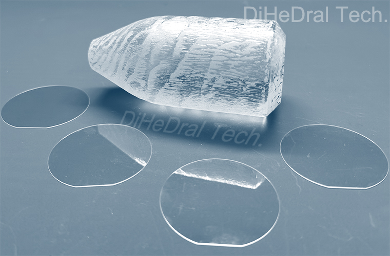
Diamond color centers can be applied in fields such as quantum information processing, biomarkers, sensitive magnetic field detection, and nanoscale heat transfer control. Electronic grade diamond can be an ideal material for electronic devices under extreme conditions such as high temperature, high frequency, high power, and radiation environment. Extremely high thermal conductivity, used as a heat sink material for high-power devices such as LEDs, lasers, and chips.

Silicon (Si)

Silicon(Si) single crystal is one of the most widely used materials in the modern semiconductor industry, and its superior performance and cost advantages make it dominant in many applications. Silicon single crystals have a high purity and are able to form a perfect lattice structure, which is essential for manufacturing high-efficiency, low-power microelectronic devices. Silicon single crystals also exhibit good thermal and chemical stability, which allows them to operate stably in harsh envir

Germanium (Ge)

Germanium single crystals have a smaller band gap than silicon, which makes it have higher carrier mobility at room temperature and can therefore operate at higher frequencies. At the same time, the high light absorption of germanium makes it an ideal material for the production of optoelectronic devices, such as light detectors in optical fiber communication. However, the high production cost of germanium limits its use in large-scale applications, but germanium single crystals still have great

Gallium oxide (Ga2O3)

Gallium oxide (Ga2O3) is a semiconductor material with good chemical and thermal stability. Its bandgap width is 4.7-4.9 eV, critical breakdown field strength is 8 MV/cm (much higher than the theoretical limit of 2.5 MV/cm for SiC and 3.3 MV/cm for GaN), electron mobility is 250 cm2/V • s, and it has strong transparent conductivity. The Barigard value exceeds 3000, which is several times that of GaN and SiC materials.

Gallium nitride (GaN)

Gallium nitride (GaN) is a wide bandgap semiconductor material with excellent properties such as high electron mobility, high thermal conductivity and high radiation resistance. GaN is widely used in LED lamp manufacturing, RF applications, power electronics and solar cells. Especially in the field of power electronics, GaN is regarded as an important material for future power systems because it can withstand higher voltages and temperatures. At the same time, the radiation resistance properties

Silicon carbide (SiC)

Silicon carbide SiC crystal is a wide bandgap semiconductor material with excellent thermal conductivity and high electric field breakdown strength, which makes it have significant performance advantages in harsh environments such as high power, high frequency and high temperature. SiC crystals are widely used in power electronic equipment, such as power devices in electric vehicles, rail transit, power grids and other fields, and can also be used as materials for high-temperature, high-frequenc

Gallium arsenide (GaAs)

GaAs crystal is a direct bandgap semiconductor material with good electron migration performance and high electron velocity, which is suitable for high-speed electronic devices. Compared to silicon, GaAs is better suited to manufacturing faster electronics. In addition, GaAs crystals have a strong absorption capacity for light, so they are widely used in optoelectronic fields such as solar cells, photodiodes, and laser diodes.

Indium phosphide (InP)

Indium phosphide (InP) is an important III-V semiconductor material with direct bandgap properties and high electron mobility. InP single crystal has a band gap of about 1.35 eV and excellent optical and electronic properties at room temperature. InP is often used to make high-speed electronic devices, including high-frequency, high-speed optical fiber communication systems, microwave devices, and some high-efficiency solar cells. In addition, due to the high refractive index and good thermal st

Gallium antimonide (GaSb)

GaSb is the chemical formula of gallium arsenide, an important semiconductor material. It has a wide range of applications, including infrared detectors, lasers, photoelectric sensors, etc. GaSb's outstanding properties include high electron mobility, wide bandgap, low noise, and high saturation drift speed, making it ideal for infrared technology and optoelectronics.

Indium arsenide (InAs)

InAs is the chemical formula of indium arsenide, an important semiconductor material. It has excellent electronic motion performance and optical characteristics, and is widely used in infrared detectors, photoelectric sensors, lasers and other fields. InAs offers high carrier mobility, wide bandgap adjustment range, and fast response speed, providing good performance for infrared optics and electronics.

Zinc oxide (ZnO)

ZnO is the chemical formula of zinc oxide and is a widely used semiconductor material. It has excellent optoelectronic properties and optical properties and can be used in optoelectronic devices, optical coatings, sensors, etc. The advantages of ZnO include wide bandgap, high transparency, excellent electron transport performance and good chemical stability, making it an important application value in optoelectronics and optics.

Cadmium zinc telluride (CdZnTe)

CdZnTe is the chemical formula of zinc cadmium telluride, which is an important semiconductor material. It has wide bandgap and high electron mobility and is widely used in X-ray and γ-ray detectors, nuclear medicine imaging, and other fields. The advantages of CdZnTe include high energy resolution, fast response time, and good radiation hardness, making it a key material for radiographic detection and imaging techniques.

Magnesium fluoride (MgF2)

MgF2, the chemical formula for magnesium fluoride, is an important optical material with excellent optical transparency and chemical stability. It is often used in ultraviolet optical devices, laser optical components, and optical coatings. The characteristics of MgF2 include wide wavelength range, low scattering loss, and higher refractive index, making it an important part of optical systems.

Calcium fluoride (CaF2)

CaF2, the chemical formula for calcium fluoride, is a widely used optical material with excellent optical transparency, low refractive loss, and chemical stability. It is commonly used in ultraviolet optical devices, laser optical components, and optical coatings. The advantages of CaF2 include a wide wavelength range, low scattering loss, and higher refractive index, making it an important material in the optical field.

Barium fluoride (BaF2)

BaF2, the chemical formula for barium fluoride, is an important optical material with excellent optical transparency and chemical stability. It is widely used in ultraviolet optical devices, laser optical components, and optical coatings. The characteristics of BaF2 include wide wavelength range, low scattering loss, and higher refractive index, making it an important part of optical systems.

Lithium fluoride (LiF)

LiF, the chemical formula for lithium fluoride, is an important optical material with excellent optical transparency, chemical stability, and higher refractive index. It is widely used in ultraviolet optical devices, laser optical components, and optical coatings. The advantages of LiF include wide wavelength range, low scattering loss, and higher refractive index, making it significant in the optical field.

Yttrium aluminium garnet (YAG)

YAG, the chemical formula for yttrium aluminum garnet, is an important crystal material with excellent optical and physical properties. It is widely used in lasers, optical communication, medical imaging, etc. The advantages of YAG include high hardness, excellent thermal conductivity, and good optical transparency, to: AI Assistant<

Cerium doped lutetium yttrium orthosilicate (Ce:LYSO)

Cerium-doped lutetium yttrium orthosilicate (Ce:LYSO) is an excellent scintillator with high scintillation efficiency, fast scintillation response, and longer fluorescence lifetime. It is widely used in medical imaging, particle detection, and nuclear physics experiments.

Cerium doped yttrium aluminium garnet (Ce:YAG)

Cerium-doped YAG (Ce:YAG) is an important scintillating crystal with good optical and scintillation performance.

Cerium doped yttrium aluminium perovskite (Ce:YAP)

Cerium-doped YAP (Ce:YAP) is a scintillating crystal with good optical and scintillation properties.

Bismuth germanate (BGO)

Bismuth germanate (BGO) is a commonly used scintillating crystal with excellent optical and scintillation performance.

Cadmium tungstate (CdWO4)

Cadmium tungstate (CdWO4) is an inorganic crystal material with excellent optical properties. It is widely used in the fields of lasers and optoelectronics, especially in scintillation detectors and medical imaging systems. CdWO4 scintillation crystal is famous for its high light yield, fast decay time, high density, and good energy resolution. In addition, this crystal is sensitive to X-ray and γ X-rays have excellent sensitivity, therefore they have high value in the field of radiation detecti

Rare earth doped lithium yttrium fluoride (RE:LiYF4)

Rare earth-doped lithium yttrium fluoride (RE:LiYF4) is a laser crystal with unique properties such as high laser damage threshold, large emission cross-section, and wide tuning range. It has been widely researched and optimized for laser applications in various fields.

Rare earth doped lithium lutetium fluoride (RE:LiLuF4)

Rare earth-doped lithium lutetium fluoride crystal (RE:LiLuF4) is a crystal containing rare earth elements like erbium, lutetium, or holmium. Its excellent optical and spectral performance makes it an attractive material for various applications.

Ytterbium doped yttrium aluminium garnet (Yb:YAG)

Ytterbium-doped YAG (Yb:YAG) crystal is a promising laser material, more suitable for diode-pumped laser systems than traditional Nd:YAG crystals.

Neodymium doped yttrium aluminium garnet (Nd:YAG)

Neodymium-doped YAG (Nd:YAG) crystal is the most important laser crystal, widely used in industry, medicine, and scientific research.

Erbium doped yttrium aluminium garnet (Er:YAG)

Erbium-doped YAG (Er3+:YAG) crystal is an attractive laser material for eye-safe emission at 1617 and 1645 nm wavelengths, pumped into the upper laser level at 1470 nm and 1532 nm by diode resonance.

Holmium doped yttrium aluminium garnet (Ho:YAG)

Holmium-doped YAG (Ho:YAG) crystal is one of the earliest studied 2um laser crystals. Its output wavelength is close to 2.1um, within the atmospheric window.

Lithium niobate (LiNbO3)

Lithium niobate (LiNbO3) is an important electro-optic crystal material with excellent electro-optic characteristics. It is widely used in fiber-optic communication, optical modulators, optical switches, and other fields.

Lithium tantalate (LiTaO3)

Lithium tantalate (LiTaO3) is a crystal material with excellent electro-optic properties. It is widely used in optical modulators, acousto-optic modulators, and piezoelectric sensors, among other areas.

Potassium hydrogen phthalate (KAP)

Potassium hydrogen phthalate (KAP) is an important nonlinear optical crystal. It has excellent optical properties and is ideal for applications in nonlinear optics.

Potassium titanyl phosphate (KTP)

Potassium titanyl phosphate (KTP) is an important nonlinear optical crystal. It has excellent nonlinear optical properties and is widely used in frequency doubling, optical modulation, and optical oscillation, among other areas.

Quartz (SiO2)

Quartz crystal (SiO2) is an important optical material with a wide range of applications. It plays a key role in optical devices, optical coatings, and optical communication, among other fields.

Titanium dioxide (TiO2)

Titanium dioxide (TiO2) is an important semiconductor material with a wide range of applications. It plays an important role in solar cells, photocatalysis, optoelectronic devices, and other fields.

Tellurium dioxide (TeO2)

Tellurium dioxide (TeO2) is an important optical crystal material with excellent optical properties and acousto-optic characteristics. It is widely used in acousto-optic modulators, fiber optic sensors, and optical waveguides, among other areas.

Yttrium aluminate (YAlO3)

Yttrium aluminum oxide (YAlO3) is an important crystal material with excellent optical and electrical properties. It is widely used in lasers, optical waveguides, and optical coatings, among other areas.

Tin selenide (SnSe2)

SnSe2It is a two-dimensional material, which is a semiconductor with unique physical properties. Its special electronic structure, including large band gap and high charge carrier mobility, makes it have important application potential in optoelectronics and energy fields such as photovoltaic and thermoelectric applications. In addition, it also has a wide range of applications in electronic devices, photosensors, and catalysts.

Tungsten sulfide (WS2)

WS2 is a two-dimensional material with a multilayer or monolayer structure that exhibits outstanding optoelectronic properties such as photocatalysis and photoconductivity. Its properties such as photoconductivity, corrosion resistance, and chemical stability make it promising in fields such as optoelectronics, catalysis, and biomedicine.

Tungsten selenide (WSe2)

WSe2, a two-dimensional semiconductor material whose monolayer has a direct bandgap, is ideal for low-power electronics. It is widely used in the fields of optoelectronic devices, logic circuits and photoelectric sensors.

Tungsten telluride (WTe2)

WTe2 is a two-dimensional semiconductor material with high electrical conductivity and unique magnetic properties. Furthermore, it exhibits a strong anomalous quantum Hall effect, making it a potential application in quantum computers and spintronics.

Rhenium sulfide (ReS2)

ReS2 is a 2D material that exhibits properties distinct from other transition metal dichalcogenides, such as higher cationic charge density and lower symmetry. Due to their unique optical and electronic properties,ReS2Has potential applications in optoelectronics and spintronics.

Rhenium selenide (ReSe2)

ReSe2 is a two-dimensional semiconductor material with low symmetry and excellent optical properties. Furthermore, it has wide applications in electronic devices and optoelectronic devices due to its good electron transport properties and high charge carrier mobility.

Molybdenum selenide (MoSe2)

MoSe2 is a two-dimensional semiconductor material whose bandgap width can be tuned by its thickness, endowing it with important applications in electronic and optoelectronic devices. MoSe2 exhibits excellent optoelectronic properties, optical properties, and high carrier mobility, and is widely used in optoelectronic devices, such as photodetectors, photocells, and even quantum devices. In addition, due to its excellent catalytic performance, it also has important applications in energy conversi

Iron chloride (FeCl2)

FeCl2 is a two-dimensional material that exhibits good magnetic and optical properties and thus has potential applications in magnetic memories and optoelectronic devices.

Niobium sulfide (NbS3)

NbS3 is a two-dimensional semiconductor material with low symmetry and excellent optical properties. Furthermore, it has wide applications in electronic devices and optoelectronic devices due to its good electron transport properties and high charge carrier mobility.

Gallium telluride iodide (GaTeI)

GaTeI is a two-dimensional material that exhibits excellent magnetic and optical properties, and thus has potential applications in magnetic memories and optoelectronic devices.

Indium selenide (InSe)

InSe is a two-dimensional material with excellent electronic properties, high electron mobility and good optical properties. Therefore, InSe is widely used in electronic equipment and optoelectronic devices.

Copper indium phosphide sulfide (CuInP2S6)

CuInP2S6 is a two-dimensional material, due to its low-dimensional structure, it has unique electromagnetic properties, such as high electrical conductivity and excellent optoelectronic properties, so it is widely used in the electronics and optoelectronic industries.

Tungsten sulfide selenide (WSSe)

WSSe is a two-dimensional semiconductor material with low symmetry and excellent optical properties. Furthermore, it has wide applications in electronic devices and optoelectronic devices due to its good electron transport properties and high charge carrier mobility.

Iron germanium telluride (Fe3GeTe2)

Fe3GeTe2 is a two-dimensional material that exhibits excellent magnetic and optical properties and thus has potential applications in magnetic memories and optoelectronic devices.

Nickel iodide (NiI2)

NiI2It is a two-dimensional material with excellent electronic properties, high electron mobility and good optical properties. therefore,NiI2It is widely used in electronic equipment and optoelectronic devices.

Iron phosphorus sulfide (FePS3)

FePS3 is a two-dimensional material that exhibits excellent magnetic and optical properties, and thus has potential applications in magnetic memories and optoelectronic devices.

Manganese phosphorus selenide (MnPSe3)

MnPSe3 is a two-dimensional material with excellent electronic properties, high electron mobility and good optical properties. Therefore, MnPSe3 is widely used in electronic equipment and optoelectronic devices.

Manganese phosphorus sulfide (MnPS3)

MnPS3 is a two-dimensional material with excellent optoelectronic and magnetic properties. As a material with low-dimensional magnetism, MnPS3 shows great potential in spintronics. Furthermore, its layered structure lends it potential applications in various electronic and optoelectronic devices, including optoelectronic devices, magnetic memories, and energy storage and conversion devices.

Arsenic (As)

Selenium (Se)

Tellurium (Te)

Carbon powder (C)

Scandium (Sc)

Titanium (Ti)

Indium (In)

Gallium (Ga)

Bismuth (Bi)

Tin (Sn)

Zinc (Zn)

Cadmium (Cd)

Antimony (Sb)

Copper (Cu)

Nickel (Ni)

Molybdenum (Mo)

Aluminium (Al)

Rhenium (Re)

Hafnium (Hf)

Vanadium (V)

Chromium (Cr)

Iron (Fe)

Cobalt (Co)

Zirconium (Zr)

Niobium (Nb)

Tungsten (W)

Germanium (Ge)

Barium titanate (BaTiO3)

BaTiO3 is an important ferroelectric material with excellent dielectric and piezoelectric properties. It is widely used in capacitors, sensors, piezoelectric actuators, and other areas. The advantages of BaTiO3 include a high piezoelectric coefficient, a wide range of dielectric constants, and excellent piezoelectric stability, making it an ideal material for ferroelectric and piezoelectric devices.

Strontium titanate (SrTiO3)

SrTiO3 is an important oxide material with a wide range of applications. It plays a key role in electronic devices, optoelectronic devices, superconducting materials, and other fields. The advantages of SrTiO3 include excellent dielectric performance, high electron mobility, and good thermal stability, making it the foundation of many functional materials.

Iron doped strontium titanate (Fe:SrTiO3)

Fe:SrTiO3 is a ferro-doped strontium titanate crystal with excellent electrical, optical, and magnetic properties. It is widely used in magneto-optic devices, magneto-optic storage, and magneto-optic modulators, among other areas. The advantages of Fe:SrTiO3 include adjustable electrical, optical, and magnetic properties, giving it important application prospects in multifunctional devices.

Neodymium doped strontium titanate (Nd:SrTiO3)

Nd:SrTiO3 is a neodymium-doped strontium titanate crystal with excellent optical and laser properties. It is widely used in lasers, optical amplifiers, and optical communication systems, among other areas. The advantages of Nd:SrTiO3 include a wide range of optical tuning, high laser efficiency, and excellent optical stability, making it one of the key materials in laser technology.

Aluminium oxide (Al2O3)

Al2O3, also known as alumina or corundum, is an important ceramic material. It has excellent high-temperature stability, high hardness, and chemical stability, and is widely used in ceramics, coatings, electronic devices, and other fields. The advantages of Al2O3 include excellent insulating properties, good wear resistance, and a high melting point, making it a key component in engineering materials.

Potassium tantalum oxide (KTaO3)

KTaO3 crystal is an important potassium tantalate crystal material with excellent physical and optical properties. It has good optical transparency, high electron mobility, and excellent nonlinear optical characteristics. KTaO3 crystal is widely used in optoelectronics, optical communication, optical sensors, and nonlinear optics, among other areas. Its advantages include a wide range of optical tuning, a high optical nonlinearity coefficient, and a fast optical response speed, making it one of

Lead magnesium niobate–lead titanate (PMN-PT)

PMN-PT is a composite lead magnesium titanate-iron potassium scandium crystal material with excellent piezoelectric and electrostrictive properties. It is widely used in ultrasonic transducers, acousto-optic modulators, piezoelectric actuators, and other fields. The advantages of PMN-PT include a high piezoelectric coefficient, a wide electrical coupling coefficient, and excellent mechanical properties, making it an important choice in the field of piezoelectric materials.

Magnesium oxide (MgO)

MgO, also known as magnesium oxide, is an important inorganic material. It has excellent thermal stability, electrical insulation, and chemical stability, and is widely used in ceramics, electronic devices, optical coatings, and other fields. The advantages of MgO include a high melting point, good insulation, and optical transparency, giving it a key role in multiple fields.

Magnesium aluminate spinel (MgAl2O4)

MgAl2O4 is an important spinel structure ceramic material, also known as magnesium aluminate spinel. It has excellent high-temperature stability, mechanical strength, and chemical stability, and is widely used in ceramics

Lithium aluminate (LiAlO2)

LiAlO2 is an important lithium aluminum oxide crystal material. It has excellent dielectric properties and thermal stability, and is widely used in electronic devices, solid-state batteries, optical coatings, and other fields. The advantages of LiAlO2 include high insulation, good chemical stability and adjustable electrical properties, which make it play an important role in material science and electronics.

Lanthanu m aluminate (LaAlO3)

LaAlO3 is an important perovskite structured oxide material. It has excellent dielectric properties and optical properties, and is widely used in fields such as electronic devices, optical devices, and thin film materials. The advantages of LaAlO3 include high dielectric constant, excellent thermal stability, and high refractive index, making it widely used in multiple application fields.

Lanthanu m strontium aluminate (LaSrAlO4)

LaSrAlO4 is a perovskite structured oxide crystal material with excellent dielectric and optical properties. It has extensive applications in fields such as electronic devices, optical devices, and thin film materials. The advantages of LaSrAlO4 include high dielectric constant, excellent thermal stability, and good optical transparency, making it an ideal choice for multifunctional materials.

(La,Sr)(Al,Ta)O3

(La, Sr) (Al, Ta) O3 is a composite perovskite structured oxide material with excellent dielectric properties and thermal stability. It is a relatively mature twin free perovskite crystal that is well matched with high-temperature superconductors and various oxide materials. It is expected to replace lanthanum aluminate (LaAlO3) and strontium titanate (SrTiO3) for giant magnetoelectric and superconducting devices.

Neodymium gallate (NdGaO3)

NdGaO3 is an important oxide material with excellent optical and electrical properties. It is widely used in fields such as lasers, optical waveguides, and electronic devices. The advantages of NdGaO3 include high optical transparency, excellent thermal conductivity and chemical stability, making it play an important role in the field of optical devices and optoelectronics.

Terbium gallium garnet (TGG)

TGG is an important terbium iron gadolinium crystal material with excellent magneto-optical properties. It is widely used in fields such as magneto optical modulators, optical isolators, and lasers. The advantages of TGG include large magneto-optical coefficient, wide optical transparency range, and excellent optical stability, making it an ideal choice for magneto-optical devices.

Gadolinium gallium garnet (GGG)

GGG is an important gadolinium aluminum iron garnet crystal material with excellent optical and magnetic properties. It is widely used in fields such as lasers, magneto optical storage, and magneto optical modulators. The advantages of GGG include a wide optical tuning range, high magneto-optical coefficient, and excellent thermal stability, making it have important application prospects in the fields of optics and magnetism.

Sodium chloride (NaCl)

NaCl is an important salt crystal material with a wide range of applications. It plays an important role in fields such as optical devices, biochemical experiments, and food processing. The advantages of NaCl include good optical transparency, chemical stability and adjustable refractive index, making it an important material in many fields.

Potassium bromide (KBr)

KBr is an important potassium bromide crystal material with excellent optical and thermal properties. It is widely used in fields such as optical components, infrared windows, and spectral analysis. The advantages of KBr include wide optical transparency range, excellent optical uniformity and stable chemical properties, which make it widely used in optics and spectroscopy.

Potassium chloride (KCl)

KCl is an important potassium chloride crystal material with a wide range of applications. It plays a crucial role in fields such as optical devices, infrared windows, and optical coatings. The advantages of KCl include good optical transparency, excellent thermal conductivity and chemical stability, making it widely used in many fields.

Gold (Au(T))

Gold (Au) Sputtering Targets offer exceptional electrical conductivity and resistance to corrosion and tarnish. This material is used in a variety of applications, ranging from decorative coating to advanced electronics.

Silver (Ag(T))

Silver sputtering targets are made of high purity silver, which are used extensively in PVD coating processes. The process involves high-energy ions bombarding the silver target, dislodging silver atoms in the process. These atoms then coat the substrate to form a thin film.

Platinum (Pt(T))

Platinum sputtering targets are fabricated from highly pure platinum. They are widely used in the manufacturing of microelectronics, providing a significant role in creating high-quality thin films in the semiconductor industry. • Application Scope: Microelectronics, Data storage technology, Corrosion-resistant coatings, Fuel cells, and Catalytic converters.

Palladium (Pd(T))

Palladium sputtering targets, produced from highly pure palladium, are utilized extensively in thin film deposition processes, particularly in the electronics and catalysis industries.

Ruthenium (Ru(T))

Ruthenium (Ru) sputtering targets are made from Ruthenium, a rare transition metal belonging to the platinum group of the periodic table. It has a shiny silver appearance. Sputtering targets made from Ruthenium are used in the manufacturing of high-density and high-performance memory chips in the semiconductor industry due to its excellent electrical properties.

Iridium (Ir(T))

Iridium (Ir) sputtering targets are thin, pure iridium metallic layers used in the fabrication of thin film devices. This thin film process, called sputtering, involves bombarding a solid iridium target with high-energy particles, causing atoms to be ejected from the target. The atoms then deposit onto a substrate forming a thin film. Iridium, being one of the densest and most corrosion-resistant metals, provides excellent qualities for various thin film applications.

Aluminium (Al(T))

Aluminum (Al) sputtering targets are widely used in the thin-film deposition of various material layers. Sputtering involves ejecting material from a "target" (in this case, aluminum) that is to be deposited on a substrate (such as a silicon wafer). Aluminum is a light, strong, and highly conductive metal, making it an excellent sputtering target.

Copper (Cu(T))

Copper (Cu) sputtering targets are a key material in the thin-film coating industry, primarily for their superior electrical and thermal conductivity. Composed of high purity copper, these targets are used for the fabrication of thin films in various electronic devices, enabling high-speed data transmission and efficient heat dissipation.

Titanium (Ti(T))

Titanium (Ti) sputtering targets are used in the deposition of titanium thin films. Titanium is a strong, lightweight, and highly corrosion-resistant metal. It is an ideal material for a wide range of thin film applications including semiconductors, decorative coatings, and medical devices.

Nickel (Ni(T))

Nickel (Ni) sputtering targets are primarily used in the manufacturing of thin films via physical vapor deposition (PVD). Nickel is a hard, malleable, ductile metal with high heat and electrical conductivity, making it an excellent choice for a wide range of applications.

Chromium (Cr(T))

Chromium (Cr) sputtering targets are used to deposit chromium thin films. Chromium is a hard, brittle metal known for its high melting point and corrosion resistance. It is widely used in the thin film industry for its excellent metallic properties.

Cobalt (Co(T))

Cobalt (Co) sputtering targets are used in the deposition of cobalt thin films. Cobalt is a hard, lustrous, silver-gray metal known for its magnetic properties and high temperature stability, making it an ideal material for various thin film applications.

Iron (Fe(T))

Iron (Fe) sputtering targets are used to deposit iron thin films. Iron is a strong, hard metal with magnetic properties, making it an ideal material for various thin film applications.

Manganese (Mn(T))

Manganese (Mn) sputtering targets are used in the deposition of manganese thin films. Manganese is a hard, brittle metal known for its high melting point and oxidation resistance, making it an ideal material for various thin film applications.

Zinc (Zn(T))

Zinc (Zn) sputtering targets are used to deposit zinc thin films. Zinc is a moderately reactive, blueish-white metal that tarnishes in moist air and burns in air with a bright, bluish-green flame. It is used in a variety of thin film applications.

Vanadium (V(T))

Vanadium (V) sputtering targets are used in the deposition of vanadium thin films. Vanadium is a hard, silvery-grey, ductile, and malleable transition metal. It has good resistance to corrosion and it is stable against alkalis, sulfuric and hydrochloric acid.

Tungsten (W(T))

Tungsten (W) sputtering targets are renowned for their high melting point, strength, and density. Being a versatile refractory metal, tungsten targets find their usage in a wide range of thin film applications such as microelectronics, solar cells, and decorative coatings.

Hafnium (Hf(T))

Hafnium (Hf) sputtering targets are used in the deposition of hafnium-based thin films. These targets are known for their high temperature resistance and are often used in applications such as integrated circuits, fiber optic cables, and thermal neutron absorbers in nuclear reactors.

Niobium (Nb(T))

Niobium (Nb) sputtering targets are used for depositing niobium-based thin films. Known for their superior superconducting properties, these targets are widely used in applications such as superconducting magnets, electronic devices, and optical coatings.

Molybdenum (Mo(T))

Molybdenum (Mo) sputtering targets are known for their high melting point and excellent thermal and electrical conductivity. They find widespread use in the electronics industry, particularly in the manufacture of thin-film transistors, integrated circuits, and solar cells.

Lanthanu m (La (T))

Lanthanu m (La) sputtering targets are used for depositing lanthanu m-based thin films. They are known for their high refractive index and are used in a variety of applications such as optical coatings, phosphors, and catalysts.

Cerium (Ce (T))

Cerium (Ce) sputtering targets are used for depositing cerium-based thin films. Known for their excellent oxidation resistance, these targets are used in a wide array of applications, including catalysts, optical coatings, and fuel cells.

Praseodymium (Pr (T))

Praseodymium sputtering targets are used for depositing praseodymium-based thin films. They are usually applied in the production of color glasses and ceramics, magnet alloys, and certain types of steel.

Neodymium (Nd (T))

Neodymium sputtering targets are utilized in the production of Neodymium-based thin films. The applications often include color glasses, lasers, and magnet alloys.

Samarium (Sm (T))

Samarium sputtering targets are used for the deposition of Samarium-based thin films. They find applications in the production of magnets, lasers, and nuclear reactors.

Europium (Eu (T))

Europium sputtering targets are used for depositing Europium-based thin films. Their applications include phosphors, lasers, and nuclear reactors.

Gadolinium (Gd (T))

Gadolinium sputtering targets are used for the deposition of Gadolinium-based thin films. They find application in magnetic resonance imaging (MRI), computer memory, and shielding in nuclear reactors.

Terbium (Tb (T))

Terbium sputtering targets are used for depositing Terbium-based thin films. They are widely used in phosphors, magnets, and lasers.

Dysprosium (Dy (T))

Dysprosium sputtering targets are used for the deposition of Dysprosium-based thin films. They find extensive application in the production of lasers, magnets, and nuclear reactors.

Holmium (Ho (T))

Holmium sputtering targets are used for depositing Holmium-based thin films. They are applied in the manufacturing of magnets, lasers, and medical devices.

Erbium (Er (T))

Erbium sputtering targets are used for depositing Erbium-based thin films. They find applications in lasers, especially fiber-optic communication systems, and medical devices.

Thulium (Tm (T))

Thulium sputtering targets are used for depositing Thulium-based thin films. They are used in the production of lasers, particularly portable X-ray machines, and medical devices.

Ytterbium (Yb (T))

Ytterbium sputtering targets are used for depositing Ytterbium-based thin films. They find applications in lasers, chemical reactions catalysts, and stainless steel.

Lutetium (Lu (T))

Lutetium sputtering targets are used for depositing Lutetium-based thin films. They are widely used in the production of phosphors, PET scanners, and catalysts.

Nickel-Iron (NiFe(T))

The NiFe sputtering target is a blend of Nickel (Ni) and Iron (Fe). Its production involves high-purity materials, stringent manufacturing controls, and comprehensive testing procedures. It is highly dense, conductive, and has a uniform microstructure, making it optimal for thin film deposition in sputtering systems. Its application primarily includes magnetic devices and anti-corrosion coatings.

Nickel-Vanadium (NiV(T))

The Nickel-Vanadium (NiV) sputtering target is a combination of Nickel (Ni) and Vanadium (V). It is known for its high sputtering yield and low impurity levels. The NiV target finds applications in the production of energy storage devices and electrochemical capacitors.

Nickel-Chromium (NiCr(T))

The Nickel-Chromium (NiCr) sputtering target consists of Nickel (Ni) and Chromium (Cr). It is a critical resource for producing thin films in microelectronics and other industries due to its heat resistance and electrical properties.

Aluminum-Silicon-Copper (AlSiCu(T))

The Aluminium Silicon Copper (AlSiCu) sputtering target combines the characteristics of aluminium, silicon, and copper. This target is utilized extensively in the semiconductor industry due to its excellent electrical and thermal properties. The AlSiCu target helps in producing high-quality thin films that are integral in several high-tech devices.

Titanium-Zirconium (TiZr(T))

The Titanium Zirconium (TiZr) sputtering target is an alloy of Titanium (Ti) and Zirconium (Zr). Known for its high melting point and superior corrosion resistance, this target finds applications in the manufacturing of hard coatings and biomedical devices.

Tungsten-Titanium (WTi(T))

The Tungsten Titanium (WTi) sputtering target comprises Tungsten (W) and Titanium (Ti). Known for its excellent hardness and high melting point, the WTi target is primarily used in the production of thin films in the electronics industry.

Carbon (C(T))

Carbon (C) sputtering targets are renowned for their excellent electrical and thermal conductivity. They are used in various applications, including microelectronics and hard coating industries.

Silicon (Si(T))

Silicon (Si) sputtering targets are known for their high purity and versatility, making them ideal for semiconductor, solar cell, and thin film applications.

Germanium (Ge(T))

Germanium (Ge) sputtering targets are notable for their high purity and excellent thermal properties. They are extensively used in the manufacture of semiconductors and infrared optical devices.

Boron (B(T))

Boron (B) sputtering targets exhibit unique chemical and physical properties, which make them well-suited for applications in semiconductor devices and nuclear technology.

Antimony (Sb(T))

Antimony (Sb) sputtering targets are valued for their unique properties such as their low thermal conductivity and brittleness. They find applications in the electronics industry and photovoltaic materials.

Tellurium (Te(T))

Tellurium (Te) sputtering targets are known for their high conductivity and find use in the fabrication of semiconductors, thermoelectric devices, and photovoltaic cells.

Aluminum Oxide (Al2O3(T))

Aluminum oxide (Al2O3) sputtering targets are renowned for their hardness and resistant nature. Their high purity levels make them suitable for use in various optical, electronic, and structural applications.

Silicon Dioxide (SiO2(T))

Silicon dioxide (SiO2) sputtering targets are widely known for their high purity and versatility, making them ideal for various applications like semiconductor devices, microelectronics, and optical applications.

Titanium Dioxide (TiO2(T))

Titanium dioxide (TiO2) sputtering targets are notable for their chemical stability and high refractive index. They find use in applications like optical coatings, solar cells, and photocatalysis.

Chromium Oxide (Cr2O3(T))

Chromium(III) oxide (Cr2O3) sputtering targets are known for their corrosion resistance and thermal stability, making them ideal for applications such as data storage, decorative coatings, and solar cells.

Nickel Oxide (NiO(T))

Nickel(II) oxide (NiO) sputtering targets are frequently used in various electronic applications due to their excellent electrical and magnetic properties. They have high purity and are perfect for producing high-quality films.

Copper Oxide (CuO(T))

Copper(II) oxide (CuO) sputtering targets are used widely in semiconductors and other electronic devices due to their superior electrical properties. They have high thermal conductivity and are resistant to corrosion.

Zinc Oxide (ZnO(T))

Zinc Oxide (ZnO) sputtering targets are widely recognized in the deposition of high-quality ZnO films, boasting excellent electrical and optical properties. They find extensive application in the manufacture of thin film transistors, solar cells, and LEDs.

Zirconium Oxide (ZrO2(T))

Zirconium Dioxide (ZrO2) sputtering targets are known for their high melting points, and outstanding resistance to corrosion and wear. They are widely utilized in the manufacturing of ceramic capacitors and fuel cells.

Indium Tin Oxide (ITO(T))

Indium Tin Oxide (ITO) sputtering targets are highly valued in the industry for their outstanding electrical conductivity and transparency to visible light, making them the ideal choice for creating transparent conducting films. They're extensively utilized in applications such as flat-panel displays, smart windows, polymer-based electronics, and thin-film solar cells.

Indium Zinc Oxide (IZO(T))

Indium Zinc Oxide (IZO) sputtering targets are prized for their high electrical conductivity and optical transparency, which makes them particularly suitable for applications in the optoelectronic industry, such as flat panel displays and thin-film solar cells.

Aluminum Doped Zinc Oxide (AZO(T))

The Aluminum-doped Zinc Oxide (AZO) sputtering target is a coveted product in the electronic industry due to its favorable electrical conductivity and optical transparency. It is also less costly and less scarce compared to ITO, making it an attractive alternative for similar applications such as transparent conducting films.

Cerium Oxide (CeO2(T))

Cerium Dioxide (CeO2) sputtering targets are renowned for their capacity to produce high-quality thin films used in the production of ceramics and catalysts. The high purity of these targets ensures a consistent and uniform film.

Tungsten Trioxide (WO3(T))

Tungsten Trioxide (WO3) sputtering targets are useful in producing high-purity thin films used in photovoltaics and electrochromic devices due to their superior electrical conductivity and optical properties. These targets enable efficient deposition and uniformity, which are critical in various applications.

Hafnium Oxide (HfO2(T))

Hafnium Dioxide (HfO2) sputtering targets offer excellent corrosion resistance and stability, making them ideal for producing thin films in semiconductor devices. These targets are essential for advanced applications due to their high refractive index and low absorption coefficient at various wavelengths.

Indium Gallium Zinc Oxide (IGZO(T))

Indium Gallium Zinc Oxide (IGZO) sputtering targets are known for their superior mobility and transparency, which are vital in the fabrication of thin-film transistors (TFTs). These targets also possess low off-state current and high on/off current ratio, enhancing device performance.

Boron Nitride (BN(T))

Boron nitride (BN) sputtering targets are used in the deposition of hard, lubricious, and chemical-resistant boron nitride films. These targets are known for their high purity, uniform grain structure, and optimal deposition rates.

Aluminum Nitride (AlN(T))

Aluminum nitride (AlN) sputtering targets are highly valued for their excellent thermal conductivity and electrical insulation properties. They are widely used in the production of electronic devices, such as power modules, LEDs, and microwave components.

Silicon Nitride (Si3N4(T))

Silicon nitride (Si3N4) sputtering targets are widely used for the deposition of thin films with excellent mechanical and thermal properties. They find applications in the production of cutting tools, wear-resistant coatings, and protective films due to their high hardness and chemical resistance.

Titanium Nitride (TiN(T))

Titanium nitride (TiN) sputtering targets are widely utilized for the deposition of hard and wear-resistant coatings. They find applications in the aerospace, automotive, and cutting tool industries due to their exceptional hardness, high melting point, and excellent adhesion.

Zirconium Nitride (ZrN(T))

Zirconium nitride (ZrN) sputtering targets are valued for their exceptional hardness, thermal stability, and resistance to wear and corrosion. They are extensively used in the production of decorative coatings, cutting tools, and wear-resistant components.

Tantalum Nitride (TaN(T))

Tantalum nitride (TaN) sputtering targets are known for their exceptional thermal and chemical stability, making them suitable for various high-temperature applications. They are widely used in the production of barrier layers, diffusion barriers, and metal contacts in semiconductor devices.

Iron Sulfide (FeS(T))

Iron(II) sulfide (FeS) sputtering targets are utilized for the deposition of thin films with desirable magnetic and optical properties. They find applications in magnetic storage devices, sensors, and optoelectronic devices.

Zinc Sulfide (ZnS(T))

Zinc sulfide (ZnS) sputtering targets are valued for their wide bandgap and excellent optical properties. They are widely used in the production of optoelectronic devices, including LEDs, photovoltaic cells, and display panels.

Copper Sulfide (CuS(T))

Copper(I) sulfide (CuS) sputtering targets are used in the deposition of thin films with desirable electrical and optical properties. They find applications in solar cells, sensors, and catalysts due to their excellent conductivity and light absorption capabilities.

Gallium Sulfide (Ga2S3(T))

Gallium sulfide (Ga2S3) sputtering targets are utilized in the deposition of thin films with excellent electrical and optical properties. They find applications in photodetectors, solar cells, and optoelectronic devices due to their wide bandgap and high photoresponsivity.

Indium Sulfide (In2S3(T))

Indium sulfide (In2S3) sputtering targets are valued for their remarkable optical properties and photoelectric conversion efficiency. They are extensively used in the production of thin-film solar cells, photodetectors, and optoelectronic devices.

Molybdenum Sulfide (MoS2(T))

Molybdenum disulfide (MoS2) sputtering targets are widely recognized for their exceptional electrical, thermal, and lubricating properties. They find applications in electronics, catalysis, and lubrication due to their unique layered structure and semiconducting behavior.

Antimony Sulfide (SbS3(T))

Antimony(III) sulfide (Sb2S3) sputtering targets are used for the deposition of thin films with desirable optoelectronic properties. They find applications in solar cells, photodetectors, and sensors due to their excellent light absorption capabilities and suitable bandgap.

Tin Sulfide (SnS(T))

Tin(II) sulfide (SnS) sputtering targets are valued for their remarkable electrical and optical properties. They find applications in solar cells, photodetectors, and thermoelectric devices due to their suitable bandgap and high absorption coefficient.

Cadmium Sulfide (CdS(T))

Cadmium sulfide (CdS) sputtering targets are extensively used for the deposition of thin films with excellent electrical and optical properties. They find applications in solar cells, photodetectors, and optoelectronic devices due to their suitable bandgap and high photoresponsivity.

Copper Zinc Tin Sulfide (Cu2ZnSnS4(T))

Copper zinc tin sulfide (Cu2ZnSnS4) sputtering targets are highly valued for their excellent light absorption properties and suitable bandgap, making them ideal for thin-film solar cell applications. They have gained significant attention as a potential absorber material due to their earth-abundant and environmentally friendly composition.

Magnesium Boride (MgB2(T))

Magnesium diboride (MgB2) sputtering targets are widely recognized for their superconducting properties at relatively high temperatures, making them valuable for various superconducting applications. They are used in the production of superconducting thin films, wires, and devices for use in energy transmission, medical imaging, and quantum computing.

Lanthanu m Hexaboride (LaB6(T))

Lanthanu m hexaboride (LaB6) sputtering targets are highly valued for their exceptional electron emission properties, making them suitable for electron sources in electron microscopes and other electron beam applications. They exhibit a low work function, high melting point, and excellent thermionic emission, ensuring stable and efficient electron emission.

Titanium Diboride (TiB2(T))

Titanium diboride (TiB2) sputtering targets are widely used for the deposition of wear-resistant and corrosion-resistant coatings. They find applications in cutting tools, molds, and protective coatings due to their exceptional hardness, high melting point, and chemical stability.

Zinc Selenide (ZnSe(T))

Zinc selenide (ZnSe) sputtering targets are valued for their excellent optical properties and wide bandgap. They find applications in optoelectronic devices, infrared optics, and laser components due to their transparency in the infrared region and efficient light emission.

Zinc Antimonide (Zn4Sb3(T))

Zinc antimonide (Zn4Sb3) sputtering targets are used for the deposition of thin films with desirable thermoelectric properties. They find applications in thermoelectric devices, such as power generators and coolers, due to their excellent electrical conductivity and high thermoelectric efficiency.

Cadmium Selenide (CdSe(T))

Cadmium selenide (CdSe) sputtering targets are widely used for the deposition of thin films with excellent optical and electrical properties. They find applications in solar cells, photodetectors, and optoelectronic devices due to their suitable bandgap and high photoresponsivity.

Indium Telluride (In2Te3(T))

Indium telluride (In2Te3) sputtering targets are highly valued for their unique electronic and thermal properties. They find applications in phase-change memory devices, thermoelectric devices, and infrared detectors due to their high electrical conductivity and excellent thermal stability.

Tin Selenide (SnSe(T))

Tin selenide (SnSe) sputtering targets are utilized for the deposition of thin films with excellent thermoelectric properties. They find applications in thermoelectric devices, such as power generators and solid-state refrigeration, due to their high thermoelectric efficiency and suitable bandgap.

Germanium Antimonide (GeSb(T))

Germanium antimony (GeSb) sputtering targets are widely used for the deposition of thin films with exceptional phase-change properties. They find applications in phase-change memory devices and data storage due to their reversible and rapid phase transitions between amorphous and crystalline states.

Antimony Selenide (Sb2Se3(T))

Antimony(III) selenide (Sb2Se3) sputtering targets are valued for their unique electronic and optical properties. They find applications in photovoltaic devices, sensors, and optoelectronic devices due to their suitable bandgap and high photoresponsivity.

Antimony Telluride (Sb2Te3(T))

Antimony(III) telluride (Sb2Te3) sputtering target is a compound composed of antimony and tellurium elements. It is widely recognized for its unique electronic and thermal properties, making it highly valuable in various electronic and optoelectronic applications. Sb2Te3 is a topological insulator that exhibits excellent electrical conductivity in its surface states while being an insulator in the bulk. This property opens up possibilities for utilizing Sb2Te3 in spintronic devices, thermoelectr

Bismuth Telluride (Bi2Te3(T))

Bismuth telluride (Bi2Te3) sputtering targets are widely recognized for their exceptional thermoelectric properties. They find applications in thermoelectric cooling and power generation devices due to their high thermoelectric efficiency and low thermal conductivity.

Gallium Indium Tin Zinc (GaInSnZn)

Gallium Indium Tin Zinc Silver (GaInSnZnAg)

Gallium Indium Tin Silver (GaInSnAg)

Gallium Indium Tin (GaInSn)

Gallium Indium Tin Zinc-P (GaInSnZn-P)

Gallium Indium Tin Zinc-U (GaInSnZn-U)

Bismuth Tin Indium (BiSnIn)

Bismuth Tin Indium Zinc (BiSnInZn)

Bismuth Tin Indium Silver (BiSnInAg)

Tungsten Trioxide (WO3)

Hafnium Dioxide (HfO2)

Ytterbium Oxide (Yb2O3)

Erbium Oxide (Er2O3)

Lanthanu m Oxide (La2O3)

Cerium Dioxide (CeO2)

Tin Dioxide (SnO2)

Niobium Oxide (Nb2O3)

Zirconium Dioxide (ZrO2)

Zinc Oxide (ZnO)

Copper Oxide (CuO)

Magnetite (Fe3O4)

Titanium Dioxide (TiO2)

Samarium (III) oxide (Sm2O3)

Silicon Dioxide (SiO2)

Aluminum Oxide (Al2O3)

Copper Sulfide (CuS)

Zinc Sulfide (ZnS)

Antimony Sulfide (SbS)

Molybdenum Disulfide (MoS2)

Tin Disulfide (SnS2)

Tungsten Disulfide (WS2)

Boron Nitride (BN)

Aluminum Nitride (AlN)

Silicon Nitride (SiN)

Titanium Nitride (TiN)

Vanadium Nitride (VN)

Magnesium Nitride (MgN)

Zirconium Nitride (ZrN)

Hafnium Nitride (HfN)

Lithium Fluoride (LiF)

Calcium Fluoride (CaF2)

Barium Fluoride (BaF2)

Magnesium Fluoride (MgF2)

Aluminum Fluoride (AlF3)

Lanthanu m Fluoride (LaF3)

Yttrium Fluoride (YF3)

Ytterbium Fluoride (YbF3)

Sodium Hexafluoroaluminate (Na3Al3F6)

Boron Carbide (BC)

Silicon Carbide (SiC)

Titanium Carbide (TiC)

Vanadium Carbide (VC)

Molybdenum Carbide (MoC)

Niobium Carbide (NbC)

Hafnium Carbide (HfC)

Tantalum Carbide (TaC)

Gallium Chloride (GaCl3)

Indium Chloride (InCl3)

Aluminum Chloride (AlCl3)

Bismuth Chloride (BiCl3)

Cadmium Chloride (CdCl2)

Chromium Chloride (CrCl2)

Chromium Chloride Hydrate (CrCl2(H2O)n)

Copper Chloride (CuCl)

Copper Chloride II (CuCl2)

Cesium Chloride (CsCl)

Europium Chloride (EuCl3)

Europium Chloride Hydrate (EuCl3.xH2O)

Magnesium Chloride (MgCl2)

Sodium Chloride (NaCl)

Nickel Chloride (NiCl2)

Indium Chloride (InCl3)

Indium Nitrate Hydrate (In(NO3).xH2O)

Rubidium Chloride (RbCl3)

Antimony Chloride (SbCl3)

Samarium Chloride (SmCl3)

Samarium Chloride Hydrate (SmCl3.xH2O)

Scandium Chloride (ScCl3)

Tellurium Chloride (TeCl3)

Tantalum Chloride (TaCl5)

Tungsten Chloride (WCl6)

Aluminum Bromide (AlBr3)

Barium Bromide (BaBr2)

Cobalt Bromide (CoBr2)

Cadmium Bromide (CdBr2)

Gallium Bromide (GaBr3)

Gallium Bromide Hydrate (GaBr3.xH2O)

Nickel Bromide (NiBr2)

Potassium Bromide (KBr)

Lead Bromide (PbBr2)

Zirconium Bromide (ZrBr2)

Bismuth Bromide (BiBr4)

Bismuth Iodide (BiI3)

Calcium Iodide (CaI2)

Gadolinium Iodide (GdI2)

Cobalt Iodide (CoI2)

Cesium Iodide (CsI)

Europium Iodide (EuI2)

Lithium Iodide (LiI)

Lithium Iodide Hydrate (LiI.xH2O)

Gallium Iodide (GaI3)

Gadolinium Iodide (GdI3)

Indium Iodide (InI3)

Potassium Iodide (KI)

Lanthanu m Iodide (LaI3)

Lutetium Iodide (LuI3)

Magnesium Iodide (MgI2)

Sodium Iodide (NaI)

Gallium Oxide epitaxial wafer (Ga2O3)

ε - Gallium Oxide (Ga2O3)

Due to its polarization characteristics, high breakdown electric field, and wide bandgap, ε - Ga ₂ O3 has become an ideal material for high-frequency and high-power electronic devices.

Indium Tin Oxide (ITO)

Fluorine-doped Tin Oxide (FTO)

Platinum/Titanium/Silicon Dioxide/Silicon epitacial wafer (Pt/Ti/SiO2/Si)

Aluminum Oxide ceramic (Al2O3(ceramic))

Silicon Nitride ceramic (Si3N4(ceramic))

Aluminum Nitride ceramic (AlN(ceramic))

Yttria-stabilized zirconia (YSZ)

Aluminum Nitride (AlN) crystal/substrate/film

Aluminum nitride (AlN), with a wide band gap (6.2eV), ultra-high breakdown voltage, and perfect lattice match with high aluminum content AlGaN epitaxial layer, can be widely used in deep ultraviolet detectors, semiconductor laser, and high power microwave devices.

Lithium niobate thin film epitaxial wafer

Lithium niobate thin film is a thin film made of lithium niobate (LiNbO Å) material, which has many excellent properties, making it widely used in the fields of electronics, optics, and communication.

Lithium tantalate thin film epitaxial wafer

Lithium tantalate thin film is a thin film made of lithium tantalate (LiTaO3) material. LiTaO3 is a crystal material with unique electrical properties, commonly used in the manufacturing of piezoelectric and optical devices.

Aluminum

Aluminum single crystal, as an excellent material, has a wide range of applications in aviation, automotive, electronics, construction, and packaging due to its lightweight, high-strength, excellent conductivity, thermal conductivity, and corrosion resistance. Its important position in modern industry and life cannot be ignored.

Copper single crystal

Copper single crystal refers to its crystal structure consisting entirely of copper atoms, without grain boundaries or grain boundary slip, thus possessing excellent physical, chemical, and mechanical properties. It is usually prepared by high-purity melting method or single crystal growth technology. Copper single crystals have important application value in fields such as microelectronics, semiconductors, optics, and materials science.

Yttrium stabilized zirconia YSZ ceramic tube

8% mol. Yttrium stabilized zirconia (8YSZ, YSZ-8) is a high-temperature refractory ceramic material composed of 8% yttrium stabilized zirconia. 8YSZ can be used for dental restoration, turbine blade structural ceramics, bulletproof and armor ceramics, as well as ion conductive applications such as fuel cell electrolytes. Various surface areas can be generated.

InGaAs epitaxial wafer

Produce high-performance and high-quality compound semiconductor materials based on gallium arsenide (GaAs), indium phosphide (InP), and indium antimonide (GaSb) substrates.

Gallium Oxide Ga2O3(Powder)

The raw material of high-purity gallium oxide powder is white triangular crystalline particles. It can be used to produce gallium oxide single crystals, gadolinium gallium garnet, semiconductor luminescent materials, solar energy, and special glass, and can also be used as metallurgical additives. Dihedron provides high-purity Ga2O3 raw material powders from different sources, both domestically and internationally.

Gallium Nitride(GaN) epitaxial wafer

GaN epitaxial wafers are a key semiconductor material commonly used for manufacturing high-frequency, high-power, and high-temperature electronic devices, such as high electron mobility transistors (HEMTs) and optoelectronic devices. Gallium nitride has many excellent properties, including high electron mobility, high breakdown electric field strength, excellent thermal stability, and low impurity concentration.

Epitaxial silicon wafer

Silicon epitaxial wafers are commonly used in the field of semiconductor manufacturing, especially in integrated circuit manufacturing. Through epitaxial technology, different silicon layers can be achieved on the same silicon wafer, each with different electrical characteristics. This helps to integrate devices with different functions on the same chip, improving integration and performance.

Yttrium Iron Garnet(YIG) epitaxial wafers

YIG (Yttrium Iron Garnet) belongs to the garnet family. Its chemical formula is Y3Fe5O12, where Y represents yttrium atom, Fe represents iron atom, and O represents oxygen atom. YiG has magnetic and optical properties and is widely used in the fields of optical and microwave devices.

Fullerenes&Fullerols

The molecular structure of C60 is a spherical 32hedron, consisting of 60 carbon atoms connected by 20 hexagonal and 12 pentagonal rings, forming a spherical hollow symmetric molecule with 30 carbon carbon double bonds. Therefore, fullerene is also known as football.

Ce:CLLB crystal

CLLB is one of the brightest elpasolite crystals with the light yield at least twice as high as that of CLYC (up to 55,000 ph/MeV). Superior proportionality and high light yield leads the best crystals to the excellent 2.9% energy resolution at 662 keV (approaching LaBr3:Ce) and fast decay time. The selected compositions contain Li-6 ions, CLLB:Ce crystal shows thermal neutron detection efficiency (FOM≥1.5).

Iron(Fe)

Pig iron is a primary product obtained when extracting iron ore from blast furnaces. It has a high carbon content, usually between 2% and 4%, and also contains impurities such as silicon, manganese, phosphorus, and sulfur. Pig iron has high hardness and brittleness, making it unsuitable for forging, but it can be used for casting.

Iceland Spar

Iceland stone, with a chemical composition of CaCO3, is a colorless, transparent, and pure calcite. Due to its special physical properties, it is called a special non-metallic mineral. It was first discovered in Iceland, hence it is called "Iceland Stone". It has the highest birefringence and polarization performance in white transparent crystal minerals. The crystals of high-quality ice spar are produced in the calcite veins of basalt and zeolite calcite veins.

Gallium Selenide GaSe

GaSe is an important material in the fields of optoelectronics and nonlinear optics. It is a layered semiconductor material with a hexagonal crystal structure, where Ga and Se atoms are alternately arranged in each layer, and weak van der Waals forces bind the layers together. This structure makes GaSe easy to peel off into thin sheets.

Ag activated phosphate glass

Ag activated phosphate glass is a highly sensitive radiogenic material. Widely used in the fields of radiation detection, medical imaging, and industrial non-destructive testing. Compared to traditional dosage The phosphate glass dosimeter has high sensitivity, wide range, anti-interference, stable performance, long-lasting dose information storage, and can be repeatedly measured and read, and is gradually becoming the mainstream product of dosimeters.

Nd,Yb,Er,Tm,Ho,Cr,Lu Infrared laser crystal

Infrared laser crystals are a special type of crystal material that can generate laser radiation in the infrared light band (usually 1 to 100 microns). These crystals are usually composed of certain rare earth elements such as thulium, erbium, ytterbium, holmium, chromium, etc.

Spherical, irregular, flat, prism processing, coating

DHD provides a variety of customized processing services related to optical crystals, glass, ceramics, and metal materials. Such as crystal growth, single crystal thin film epitaxy, cutting, grinding, polishing, optical component processing and coating, extreme ultraviolet optical coating, ceramic product firing and processing, etc.

Dihedral (Shanghai) Science and Technology Co., Ltd is a technology-based enterprise that integrates materials, raw materials, equipment, analysis and testing, and technology services.

The company focuses on the research and development of products such as semiconductors, functional crystals, new types of glass, ceramic materials, high-purity elements, and compounds, providing optimized solutions for research and development in multiple fields.

The company is also committed to developing various high-tech equipment, providing professional tools for universities, research institutions, and enterprise research and development centers.

The company provides professional testing, consulting and other scientific research services under the "Particle Cat" scientific research service brand, helping R&D personnel focus more on scientific research, produce high-quality innovative results more efficiently, and promote the transformation of results.

Bihedral Technology adheres to the value of "innovation is the answer", achieves customers, enhances oneself, and strives to grow into an excellent enterprise in the field of technology. In the great changes of historical technological development, we work together with partners to develop and give back to society.

FOLLOW US

Twitter
Weibo
  • Semiconductor crystal
  • Functional crystal
  • 2-D material
  • High-purity element
  • Single crystal substrate
  • Sputtering Target
  • Interface thermal conductive materials
  • Compound raw materials
  • Epitaxial Wafer/Films
  • Material testing analysis
  • Scientific research equipment
  • Material processing
  • Functional Glass
  • Fine Ceramics
Request a Contact
Request a Quote
svc@mat-mall.com
+8618916221692 (WeChat)

© Copyright Dihedral (Shanghai) Science and Technology Co., Ltd 2023. All rights reserved.

+8618916221692 (WeChat)
svc@mat-mall.com
Wechat QR