 Dihedral (Shanghai) Science and Technology Co., Ltd
- Home
-
Products
-
- Semiconductor crystal
-
Single crystal substrate
-
Multifunctional single crystal substrate
- Barium titanate (BaTiO3)
- Strontium titanate (SrTiO3)
- Iron doped strontium titanate (Fe:SrTiO3)
- Neodymium doped strontium titanate (Nd:SrTiO3)
- Aluminium oxide (Al2O3)
- Potassium tantalum oxide (KTaO3)
- Lead magnesium niobate–lead titanate (PMN-PT)
- Magnesium oxide (MgO)
- Magnesium aluminate spinel (MgAl2O4)
- Lithium aluminate (LiAlO2)
- Lanthanu m aluminate (LaAlO3)
- Lanthanu m strontium aluminate (LaSrAlO4)
- (La,Sr)(Al,Ta)O3
- Neodymium gallate (NdGaO3)
- Terbium gallium garnet (TGG)
- Gadolinium gallium garnet (GGG)
- Sodium chloride (NaCl)
- Potassium bromide (KBr)
- Potassium chloride (KCl)
-
Multifunctional single crystal substrate
-
Functional crystal
- Optical window
- Scintillation crystal
-
Laser crystal
- Rare earth doped lithium yttrium fluoride (RE:LiYF4)
- Rare earth doped lithium lutetium fluoride (RE:LiLuF4)
- Ytterbium doped yttrium aluminium garnet (Yb:YAG)
- Neodymium doped yttrium aluminium garnet (Nd:YAG)
- Erbium doped yttrium aluminium garnet (Er:YAG)
- Holmium doped yttrium aluminium garnet (Ho:YAG)
- Nd,Yb,Er,Tm,Ho,Cr,Lu Infrared laser crystal
- N* crystal
- Metal single crystal
- Material testing analysis
- Material processing
- Scientific research equipment
-
-
Epitaxial Wafer/Films
-
Inorganic epitaxial wafer/film
- Gallium Oxide epitaxial wafer (Ga2O3)
- ε - Gallium Oxide (Ga2O3)
- Platinum/Titanium/Silicon Dioxide/Silicon epitacial wafer (Pt/Ti/SiO2/Si)
- Lithium niobate thin film epitaxial wafer
- Lithium tantalate thin film epitaxial wafer
- InGaAs epitaxial wafer
- Gallium Nitride(GaN) epitaxial wafer
- Epitaxial silicon wafer
- Yttrium Iron Garnet(YIG) epitaxial wafers
- Fullerenes&Fullerols
- ε-Gallium Oxide(Ga2O3)
- Indium Arsenide (InAs) epitaxial wafer
- InGaAs and other compound epitaxial wafers
- Periodic polarization of lithium niobate PPLN and lithium tantalate PPLT
-
Inorganic epitaxial wafer/film
- Functional Glass
- Fine Ceramics
-
2-D material
- 2-D crystal
-
Layered transition metal compound
- Iron chloride (FeCl2)
- Niobium sulfide (NbS3)
- Gallium telluride iodide (GaTeI)
- Indium selenide (InSe)
- Copper indium phosphide sulfide (CuInP2S6)
- Tungsten sulfide selenide (WSSe)
- Iron germanium telluride (Fe3GeTe2)
- Nickel iodide (NiI2)
- Iron phosphorus sulfide (FePS3)
- Manganese phosphorus selenide (MnPSe3)
- Manganese phosphorus sulfide (MnPS3)
- Interface thermal conductive materials
-
Epitaxial Wafer/Films
-
-
High-purity element
- Non-metallic
-
Metal
- Scandium (Sc)
- Titanium (Ti)
- Indium (In)
- Gallium (Ga)
- Bismuth (Bi)
- Tin (Sn)
- Zinc (Zn)
- Cadmium (Cd)
- Antimony (Sb)
- Copper (Cu)
- Nickel (Ni)
- Molybdenum (Mo)
- Aluminium (Al)
- Rhenium (Re)
- Hafnium (Hf)
- Vanadium (V)
- Chromium (Cr)
- Iron (Fe)
- Cobalt (Co)
- Zirconium (Zr)
- Niobium (Nb)
- Tungsten (W)
- Germanium (Ge)
- Iron(Fe)
-
Compound raw materials
-
Oxide
- Tungsten Trioxide (WO3)
- Hafnium Dioxide (HfO2)
- Ytterbium Oxide (Yb2O3)
- Erbium Oxide (Er2O3)
- Lanthanu m Oxide (La2O3)
- Cerium Dioxide (CeO2)
- Tin Dioxide (SnO2)
- Niobium Oxide (Nb2O3)
- Zirconium Dioxide (ZrO2)
- Zinc Oxide (ZnO)
- Copper Oxide (CuO)
- Magnetite (Fe3O4)
- Titanium Dioxide (TiO2)
- Samarium (III) oxide (Sm2O3)
- Silicon Dioxide (SiO2)
- Aluminum Oxide (Al2O3)
- Gallium Oxide Ga2O3(Powder)
- Sulfide
- Fluoride
- Nitride
- Carbide
-
Halide
- Gallium Chloride (GaCl3)
- Indium Chloride (InCl3)
- Aluminum Chloride (AlCl3)
- Bismuth Chloride (BiCl3)
- Cadmium Chloride (CdCl2)
- Chromium Chloride (CrCl2)
- Chromium Chloride Hydrate (CrCl2(H2O)n)
- Copper Chloride (CuCl)
- Copper Chloride II (CuCl2)
- Cesium Chloride (CsCl)
- Europium Chloride (EuCl3)
- Europium Chloride Hydrate (EuCl3.xH2O)
- Magnesium Chloride (MgCl2)
- Sodium Chloride (NaCl)
- Nickel Chloride (NiCl2)
- Indium Chloride (InCl3)
- Indium Nitrate Hydrate (In(NO3).xH2O)
- Rubidium Chloride (RbCl3)
- Antimony Chloride (SbCl3)
- Samarium Chloride (SmCl3)
- Samarium Chloride Hydrate (SmCl3.xH2O)
- Scandium Chloride (ScCl3)
- Tellurium Chloride (TeCl3)
- Tantalum Chloride (TaCl5)
- Tungsten Chloride (WCl6)
- Aluminum Bromide (AlBr3)
- Barium Bromide (BaBr2)
- Cobalt Bromide (CoBr2)
- Cadmium Bromide (CdBr2)
- Gallium Bromide (GaBr3)
- Gallium Bromide Hydrate (GaBr3.xH2O)
- Nickel Bromide (NiBr2)
- Potassium Bromide (KBr)
- Lead Bromide (PbBr2)
- Zirconium Bromide (ZrBr2)
- Bismuth Bromide (BiBr4)
- Bismuth Iodide (BiI3)
- Calcium Iodide (CaI2)
- Gadolinium Iodide (GdI2)
- Cobalt Iodide (CoI2)
- Cesium Iodide (CsI)
- Europium Iodide (EuI2)
- Lithium Iodide (LiI)
- Lithium Iodide Hydrate (LiI.xH2O)
- Gallium Iodide (GaI3)
- Gadolinium Iodide (GdI3)
- Indium Iodide (InI3)
- Potassium Iodide (KI)
- Lanthanu m Iodide (LaI3)
- Lutetium Iodide (LuI3)
- Magnesium Iodide (MgI2)
- Sodium Iodide (NaI)
-
Oxide
-
High-purity element
-
-
Sputtering Target
-
Metal target material
- Gold (Au(T))
- Silver (Ag(T))
- Platinum (Pt(T))
- Palladium (Pd(T))
- Ruthenium (Ru(T))
- Iridium (Ir(T))
- Aluminium (Al(T))
- Copper (Cu(T))
- Titanium (Ti(T))
- Nickel (Ni(T))
- Chromium (Cr(T))
- Cobalt (Co(T))
- Iron (Fe(T))
- Manganese (Mn(T))
- Zinc (Zn(T))
- Vanadium (V(T))
- Tungsten (W(T))
- Hafnium (Hf(T))
- Niobium (Nb(T))
- Molybdenum (Mo(T))
- Lanthanu m (La (T))
- Cerium (Ce (T))
- Praseodymium (Pr (T))
- Neodymium (Nd (T))
- Samarium (Sm (T))
- Europium (Eu (T))
- Gadolinium (Gd (T))
- Terbium (Tb (T))
- Dysprosium (Dy (T))
- Holmium (Ho (T))
- Erbium (Er (T))
- Thulium (Tm (T))
- Ytterbium (Yb (T))
- Lutetium (Lu (T))
- Alloy target material
- Semiconductor target material
-
Oxide target material
- Aluminum Oxide (Al2O3(T))
- Silicon Dioxide (SiO2(T))
- Titanium Dioxide (TiO2(T))
- Chromium Oxide (Cr2O3(T))
- Nickel Oxide (NiO(T))
- Copper Oxide (CuO(T))
- Zinc Oxide (ZnO(T))
- Zirconium Oxide (ZrO2(T))
- Indium Tin Oxide (ITO(T))
- Indium Zinc Oxide (IZO(T))
- Aluminum Doped Zinc Oxide (AZO(T))
- Cerium Oxide (CeO2(T))
- Tungsten Trioxide (WO3(T))
- Hafnium Oxide (HfO2(T))
- Indium Gallium Zinc Oxide (IGZO(T))
- Nitride target material
- Sulfide target material
-
Antimony tellurium selenium boron target material
- Magnesium Boride (MgB2(T))
- Lanthanu m Hexaboride (LaB6(T))
- Titanium Diboride (TiB2(T))
- Zinc Selenide (ZnSe(T))
- Zinc Antimonide (Zn4Sb3(T))
- Cadmium Selenide (CdSe(T))
- Indium Telluride (In2Te3(T))
- Tin Selenide (SnSe(T))
- Germanium Antimonide (GeSb(T))
- Antimony Selenide (Sb2Se3(T))
- Antimony Telluride (Sb2Te3(T))
- Bismuth Telluride (Bi2Te3(T))
-
Metal target material
-
Sputtering Target
-
- Services
- Media
- Partner
- Contact Us
- About

- Home
- Products
- Single crystal substrate
- Multifunctional single crystal substrate
- Lithium aluminate (LiAlO2)
Lithium aluminate (LiAlO2)
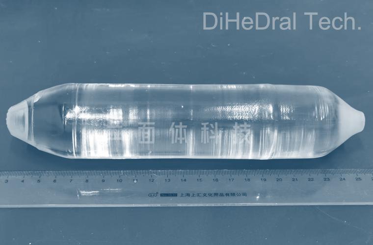

LiAlO2 (lithium aluminate) crystal is the most important substrate of High-temperature superconductivity thin films. It is well matched with High-temperature superconductivity materials such as YBaCuO, and has the characteristics of low dielectric constant and low microwave loss. LiAlO2 is a potential III-V nitride thin film substrate due to its good lattice mismatch with GaN, chemical stability at high temperatures, and more cost-effective than ZnO. LiAlO2 crystals can replace ZnO and sapphire as optical substrates. Lithium aluminate (LiAlO2) single crystal has a low lattice mismatch with GaN crystal, making it an excellent substrate for GaN thin films.
Dihedral Technology(DHD) Co., Ltd. manufacture and processing/provide multiple specifications and high quality LiAlO2 crystal,targets,materials.
Applications
LiAlO2 (lithium aluminate) crystal is the most important substrate for high-temperature superconducting thin films.
It can be used as a substrate for III-V nitride films.
LiAlO2 crystals can replace ZnO and sapphire as optical substrates.
Features
Lithium aluminate is well matched with High-temperature superconductivity materials such as YBaCuO, and has the characteristics of low dielectric constant and low microwave loss.
The chemical stability and cost-effectiveness at high temperatures are superior to zinc oxide.
Lithium aluminate (LiAlO2) single crystal has a low lattice mismatch with GaN crystal, making it an excellent substrate for GaN thin films.
-
Crystal Structure
Tetragonal
Lattice Constant
a=5.17 A c=6.26 A
Melting Point
1900℃
Density
2.62(g/cm3)
Mohs Hardness
7.5(mohs)
Mismatch Rate with GaN<001>
1.4%
Dimension
10x3mm,10x5mm,10x10mm,15x15mm,20x15mm,20x20mm
Ф15,Ф20,Ф1″,Ф2″,Ф2.6″
Thickness
0.5mm,1.0mm
Polishing
One side or two sides
Orientation
<100> <001>
Crystal Plane Orientation Accuracy
±0.5°
Edge Orientation Accuracy
2°(Special requirements can reach within 1°)
Bevel Wafer
According to specific requirements, wafers with edge-oriented crystal planes inclined at a specific angle (inclination angle 1°-45°) can be processed.
Surface Roughness
Ra≤5Å(5×5µm)
Package
Class 100 clean bag, Class 1000 super clean room