- Home
-
Products
-
- Semiconductor crystal
-
Single crystal substrate
-
Multifunctional single crystal substrate
- Barium titanate (BaTiO3)
- Strontium titanate (SrTiO3)
- Iron doped strontium titanate (Fe:SrTiO3)
- Neodymium doped strontium titanate (Nd:SrTiO3)
- Aluminium oxide (Al2O3)
- Potassium tantalum oxide (KTaO3)
- Lead magnesium niobate–lead titanate (PMN-PT)
- Magnesium oxide (MgO)
- Magnesium aluminate spinel (MgAl2O4)
- Lithium aluminate (LiAlO2)
- Lanthanu m aluminate (LaAlO3)
- Lanthanu m strontium aluminate (LaSrAlO4)
- (La,Sr)(Al,Ta)O3
- Neodymium gallate (NdGaO3)
- Terbium gallium garnet (TGG)
- Gadolinium gallium garnet (GGG)
- Sodium chloride (NaCl)
- Potassium bromide (KBr)
- Potassium chloride (KCl)
-
Multifunctional single crystal substrate
-
Functional crystal
- Optical window
- Scintillation crystal
-
Laser crystal
- Rare earth doped lithium yttrium fluoride (RE:LiYF4)
- Rare earth doped lithium lutetium fluoride (RE:LiLuF4)
- Ytterbium doped yttrium aluminium garnet (Yb:YAG)
- Neodymium doped yttrium aluminium garnet (Nd:YAG)
- Erbium doped yttrium aluminium garnet (Er:YAG)
- Holmium doped yttrium aluminium garnet (Ho:YAG)
- Nd,Yb,Er,Tm,Ho,Cr,Lu Infrared laser crystal
- N* crystal
- Metal single crystal
- Material testing analysis
- Material processing
- Scientific research equipment
-
-
Epitaxial Wafer/Films
-
Inorganic epitaxial wafer/film
- Gallium Oxide epitaxial wafer (Ga2O3)
- ε - Gallium Oxide (Ga2O3)
- Platinum/Titanium/Silicon Dioxide/Silicon epitacial wafer (Pt/Ti/SiO2/Si)
- Lithium niobate thin film epitaxial wafer
- Lithium tantalate thin film epitaxial wafer
- InGaAs epitaxial wafer
- Gallium Nitride(GaN) epitaxial wafer
- Epitaxial silicon wafer
- Yttrium Iron Garnet(YIG) epitaxial wafers
- Fullerenes&Fullerols
- ε-Gallium Oxide(Ga2O3)
- Indium Arsenide (InAs) epitaxial wafer
- InGaAs and other compound epitaxial wafers
- Periodic polarization of lithium niobate PPLN and lithium tantalate PPLT
-
Inorganic epitaxial wafer/film
- Functional Glass
- Fine Ceramics
-
2-D material
- 2-D crystal
-
Layered transition metal compound
- Iron chloride (FeCl2)
- Niobium sulfide (NbS3)
- Gallium telluride iodide (GaTeI)
- Indium selenide (InSe)
- Copper indium phosphide sulfide (CuInP2S6)
- Tungsten sulfide selenide (WSSe)
- Iron germanium telluride (Fe3GeTe2)
- Nickel iodide (NiI2)
- Iron phosphorus sulfide (FePS3)
- Manganese phosphorus selenide (MnPSe3)
- Manganese phosphorus sulfide (MnPS3)
- Interface thermal conductive materials
-
Epitaxial Wafer/Films
-
-
High-purity element
- Non-metallic
-
Metal
- Scandium (Sc)
- Titanium (Ti)
- Indium (In)
- Gallium (Ga)
- Bismuth (Bi)
- Tin (Sn)
- Zinc (Zn)
- Cadmium (Cd)
- Antimony (Sb)
- Copper (Cu)
- Nickel (Ni)
- Molybdenum (Mo)
- Aluminium (Al)
- Rhenium (Re)
- Hafnium (Hf)
- Vanadium (V)
- Chromium (Cr)
- Iron (Fe)
- Cobalt (Co)
- Zirconium (Zr)
- Niobium (Nb)
- Tungsten (W)
- Germanium (Ge)
- Iron(Fe)
-
Compound raw materials
-
Oxide
- Tungsten Trioxide (WO3)
- Hafnium Dioxide (HfO2)
- Ytterbium Oxide (Yb2O3)
- Erbium Oxide (Er2O3)
- Lanthanu m Oxide (La2O3)
- Cerium Dioxide (CeO2)
- Tin Dioxide (SnO2)
- Niobium Oxide (Nb2O3)
- Zirconium Dioxide (ZrO2)
- Zinc Oxide (ZnO)
- Copper Oxide (CuO)
- Magnetite (Fe3O4)
- Titanium Dioxide (TiO2)
- Samarium (III) oxide (Sm2O3)
- Silicon Dioxide (SiO2)
- Aluminum Oxide (Al2O3)
- Gallium Oxide Ga2O3(Powder)
- Sulfide
- Fluoride
- Nitride
- Carbide
-
Halide
- Gallium Chloride (GaCl3)
- Indium Chloride (InCl3)
- Aluminum Chloride (AlCl3)
- Bismuth Chloride (BiCl3)
- Cadmium Chloride (CdCl2)
- Chromium Chloride (CrCl2)
- Chromium Chloride Hydrate (CrCl2(H2O)n)
- Copper Chloride (CuCl)
- Copper Chloride II (CuCl2)
- Cesium Chloride (CsCl)
- Europium Chloride (EuCl3)
- Europium Chloride Hydrate (EuCl3.xH2O)
- Magnesium Chloride (MgCl2)
- Sodium Chloride (NaCl)
- Nickel Chloride (NiCl2)
- Indium Chloride (InCl3)
- Indium Nitrate Hydrate (In(NO3).xH2O)
- Rubidium Chloride (RbCl3)
- Antimony Chloride (SbCl3)
- Samarium Chloride (SmCl3)
- Samarium Chloride Hydrate (SmCl3.xH2O)
- Scandium Chloride (ScCl3)
- Tellurium Chloride (TeCl3)
- Tantalum Chloride (TaCl5)
- Tungsten Chloride (WCl6)
- Aluminum Bromide (AlBr3)
- Barium Bromide (BaBr2)
- Cobalt Bromide (CoBr2)
- Cadmium Bromide (CdBr2)
- Gallium Bromide (GaBr3)
- Gallium Bromide Hydrate (GaBr3.xH2O)
- Nickel Bromide (NiBr2)
- Potassium Bromide (KBr)
- Lead Bromide (PbBr2)
- Zirconium Bromide (ZrBr2)
- Bismuth Bromide (BiBr4)
- Bismuth Iodide (BiI3)
- Calcium Iodide (CaI2)
- Gadolinium Iodide (GdI2)
- Cobalt Iodide (CoI2)
- Cesium Iodide (CsI)
- Europium Iodide (EuI2)
- Lithium Iodide (LiI)
- Lithium Iodide Hydrate (LiI.xH2O)
- Gallium Iodide (GaI3)
- Gadolinium Iodide (GdI3)
- Indium Iodide (InI3)
- Potassium Iodide (KI)
- Lanthanu m Iodide (LaI3)
- Lutetium Iodide (LuI3)
- Magnesium Iodide (MgI2)
- Sodium Iodide (NaI)
-
Oxide
-
High-purity element
-
-
Sputtering Target
-
Metal target material
- Gold (Au(T))
- Silver (Ag(T))
- Platinum (Pt(T))
- Palladium (Pd(T))
- Ruthenium (Ru(T))
- Iridium (Ir(T))
- Aluminium (Al(T))
- Copper (Cu(T))
- Titanium (Ti(T))
- Nickel (Ni(T))
- Chromium (Cr(T))
- Cobalt (Co(T))
- Iron (Fe(T))
- Manganese (Mn(T))
- Zinc (Zn(T))
- Vanadium (V(T))
- Tungsten (W(T))
- Hafnium (Hf(T))
- Niobium (Nb(T))
- Molybdenum (Mo(T))
- Lanthanu m (La (T))
- Cerium (Ce (T))
- Praseodymium (Pr (T))
- Neodymium (Nd (T))
- Samarium (Sm (T))
- Europium (Eu (T))
- Gadolinium (Gd (T))
- Terbium (Tb (T))
- Dysprosium (Dy (T))
- Holmium (Ho (T))
- Erbium (Er (T))
- Thulium (Tm (T))
- Ytterbium (Yb (T))
- Lutetium (Lu (T))
- Alloy target material
- Semiconductor target material
-
Oxide target material
- Aluminum Oxide (Al2O3(T))
- Silicon Dioxide (SiO2(T))
- Titanium Dioxide (TiO2(T))
- Chromium Oxide (Cr2O3(T))
- Nickel Oxide (NiO(T))
- Copper Oxide (CuO(T))
- Zinc Oxide (ZnO(T))
- Zirconium Oxide (ZrO2(T))
- Indium Tin Oxide (ITO(T))
- Indium Zinc Oxide (IZO(T))
- Aluminum Doped Zinc Oxide (AZO(T))
- Cerium Oxide (CeO2(T))
- Tungsten Trioxide (WO3(T))
- Hafnium Oxide (HfO2(T))
- Indium Gallium Zinc Oxide (IGZO(T))
- Nitride target material
- Sulfide target material
-
Antimony tellurium selenium boron target material
- Magnesium Boride (MgB2(T))
- Lanthanu m Hexaboride (LaB6(T))
- Titanium Diboride (TiB2(T))
- Zinc Selenide (ZnSe(T))
- Zinc Antimonide (Zn4Sb3(T))
- Cadmium Selenide (CdSe(T))
- Indium Telluride (In2Te3(T))
- Tin Selenide (SnSe(T))
- Germanium Antimonide (GeSb(T))
- Antimony Selenide (Sb2Se3(T))
- Antimony Telluride (Sb2Te3(T))
- Bismuth Telluride (Bi2Te3(T))
-
Metal target material
-
Sputtering Target
-
- Services
- Media
- Partner
- Contact Us
- About
- Home
- Products
- Epitaxial Wafer/Films
- Inorganic epitaxial wafer/film
- InGaAs and other compound epitaxial wafers
InGaAs and other compound epitaxial wafers
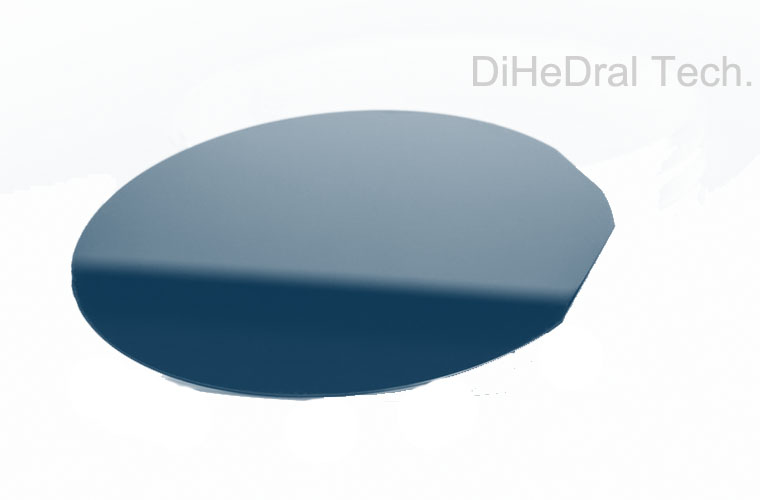
High performance and high-quality compound semiconductor materials based on gallium arsenide (GaAs), indium phosphide (InP), and indium antimonide (GaSb) substrates can cover near-infrared to long wavelength infrared spectra, becoming a "golden band" solution in the field of optoelectronics. In the future, with breakthroughs in superlattice band engineering and heterogeneous integration technology, its applications will extend to cutting-edge fields such as quantum sensing and neural morphology computing.
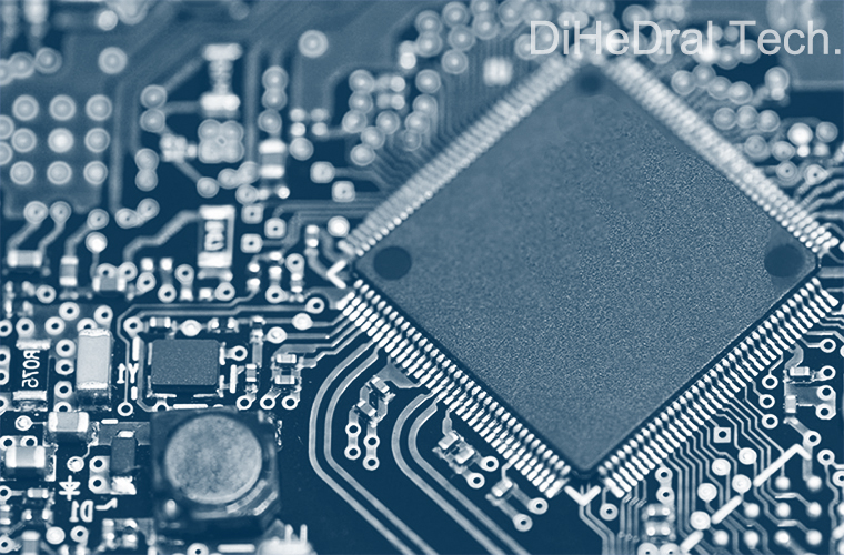
Applications
Applied to photodetectors, avalanche diodes, heterojunction bipolar transistors, quantum cascade lasers, high electron mobility transistors, etc.
Features
InGaAs (Indium Gallium Arsenide) is a III-V compound semiconductor material with many superior properties, making it widely used in the fields of optoelectronics and semiconductors. Here are some of the main advantages of InGaAs materials:
Wide bandgap adjustment range: InGaAs can achieve wide bandgap adjustment by adjusting the composition of Indium and Gallium. This enables InGaAs to cover the infrared spectral range, including near-infrared and shortwave infrared, which is crucial for many optoelectronic devices and communication applications.
High electron mobility: InGaAs has a high electron mobility, making it an ideal choice for high-speed electronic devices. This is crucial for high-frequency, high-speed applications such as high-speed field-effect transistors (FETs) and high-frequency photodetectors.
Sensitivity of photodetectors: InGaAs has high photoelectric detection sensitivity in the near-infrared and shortwave infrared ranges. This makes InGaAs photodetectors widely used in fields such as night vision, communication, and medical imaging.
High saturation drift velocity: Due to its high electron mobility, InGaAs exhibits high saturation drift velocity under high electric fields. This is very advantageous for high-frequency applications and high-speed electronic devices.
Low noise performance: InGaAs photodetectors typically exhibit low noise levels, which is crucial for applications that require high detector sensitivity and accuracy, such as optical communications and scientific instruments.
-
InGaAs PIN 光电探测器外延材料
产品规格
尺寸
2"、3"、4"
外延化合物
InP、InAlAs、InGaAs
掺杂
S i ( N 型 ) B e ( P 型 )
波段
常规波长0.9~1.7
延伸波长1.0~2.5
产品结构
平面型
材料
掺杂浓度(/cm³)
厚 度 ( n m )
InP
Substrate
InP Buffer
1-5×10¹8
200-1000
n+-In,Al1As Buffer
1-5×10¹
1000-2000
i-InGaAs Absorber
uid
1500-3000
n-In,Al₁As Cap
1-5×10¹6
500-1000
台面型
InP
Substrate
InP Buffer
1-5×10¹8
200-1000
n+-In Al₁As Buffer
1-5×10¹8
1000-2000
i-InGaAs Absorber
uid
1500-3000
p-In,Al₁₋As Cap
1-5×10¹
500-1000
InP基雪崩二极管 (APD) 外延材料
产品规格
尺寸
2"、3"、4"
外延化合物
InP、InGaAs、InGaAsP、InAlAs
掺杂
S i ( N 型 )
产品结构1
材料
掺杂浓度(/cm³)
厚度(nm)
InP
N-substrate
InP Buffer
1-5×10¹8
200-1000
InGaAs Absorber
uid
1500-3000
InGaAsP
uid
10-500
InP
1-5×10¹7
200-1000
InP
uid
2500-4000
产品结构2
材料
掺杂浓度(/cm³)
厚度(nm)
InP
N-substrate
InP Buffer
1-5×10¹⁸
200-1000
InAlAs
1-5×10¹8
200-1000
InGaAs Absorber
uid
1500-3000
InA1As
uid
10-500
InAlAs
1-5×10¹7
200-1000
InP
uid
500-4000
异质结双极晶体管 (HBT) 外延材料
产品规格
尺寸
2"、3"、4"、6"
外延化合物
GaAs、AlGaAs、InGaAs、InP
掺杂
S i ( N 型 ) B e ( P 型 )
产品结构1
材料
掺杂浓度(/cm³)
厚度(nm)
InP
N-substrate
n+InGaAs
1-5×10¹8
200-1000
p+InGaAs
10¹⁸-10¹⁹
50-150
N InP
1-5×10¹7
100-1000
n+InGaAs
1-5×10¹⁹
10-100
产品结构2
材料
掺 杂 浓 度 ( / c m ³ )
厚度(nm)
GaAs
N-substrate
n+GaAs
1-5×10¹8
200-1000
p+GaAs
10¹⁸-10¹⁹
50-150
N AlGaAs
1-5×10¹7
100-1000
n+GaAs
1-5×10¹⁹
10-100
量子级联激光器 (QCL) 外延材料
产品规格
尺寸
2"、3"、4"、6"
外延化合物
GaAs、AlGaAs、InP、InGaAs、InAlAs
掺杂
S i ( N 型 )
产 品 结 构 1
材料
掺杂浓度(/cm³)
厚 度 ( n m )
GaAs
Substrate
GaAs
1-8×10¹8
200-1000
AlGaAs
uid
5-50
数字递变层
uid
100-1000
有源区(×100 - ×200)
uid
2000-8000
数字递变层
uid
100-1000
AlGaAs
uid
5-50
GaAs
1-8×10¹8
50-150
产 品 结 构 2
材料
掺杂浓度(/cm³)
厚 度 ( n m )
InP
Substrate
InP
1-5×10¹7
200-1000
InGaAs
uid
5-50
数字递变层
1-5×10¹7
20-100
有源区(×20-×50)
uid
500-2000
数字递变层
1-5×10¹7
20-100
InP
0.1-8×10¹8
500-2000
InGaAs
1-2×10¹9
10-100
GaAs 基赝配高电子迁移率晶体管 (pHEMT) 外延材料
产品规格
尺寸
2"、3"、4"、6"
外延化合物
GaAs、AlGaAs、InGaAs
掺杂
S i ( N 型 )
产品结构
材料
掺杂浓度(/cm³)
厚度(nm)
GaAs
Substrate
GaAs Buffer
uid
50~1000
i-InGaAs
uid
10-50
i-AlGaAs
uid
1-50
δ-Si
4-5×10¹²cm-²
i-AlGaAs
uid
1-50
n-GaAs
1-8×10¹8cm³
10-200
InAs/GaSb 探测器外延材料
产品规格
尺寸
2"、3"
外延化合物
InAs、GaSb
掺杂
Si(N型)、Be(P型)、Te(N型)
产品结构1
材料
掺杂浓度(/cm³)
厚度(nm)
GaSb
Substrate
p-GaSb buffer
1-5×10¹⁸
200-1000
p-InAs/GaSb
1-5×10¹8
200-800
i-InAs/GaSb Absorber
uid
1500-4000
n-InAs/GaSb
1-5×10¹8
200-800
n-InAs
1-5×10¹⁸
10-100
产品结构2
材料
掺杂浓度(/cm³)
厚度(nm)
GaSb
Substrate
p-GaSb buffer
1-5×10¹8
200-1000
p-InAs/GaSb MW
1-5×10¹8
200-800
i-InAs/GaSb MW Absorber
uid
1500-4000
n-GaSb
1-5×10¹⁸
200-800
i-InAs/GaSb LW Absorber
uid
1500-4000
p-InAs/GaSb LW
1-5×10¹⁸
200-800
p-GaSb
1-5×10¹8
500-1000