- Home
-
Products
-
- Semiconductor crystal
-
Single crystal substrate
-
Multifunctional single crystal substrate
- Barium titanate (BaTiO3)
- Strontium titanate (SrTiO3)
- Iron doped strontium titanate (Fe:SrTiO3)
- Neodymium doped strontium titanate (Nd:SrTiO3)
- Aluminium oxide (Al2O3)
- Potassium tantalum oxide (KTaO3)
- Lead magnesium niobate–lead titanate (PMN-PT)
- Magnesium oxide (MgO)
- Magnesium aluminate spinel (MgAl2O4)
- Lithium aluminate (LiAlO2)
- Lanthanu m aluminate (LaAlO3)
- Lanthanu m strontium aluminate (LaSrAlO4)
- (La,Sr)(Al,Ta)O3
- Neodymium gallate (NdGaO3)
- Terbium gallium garnet (TGG)
- Gadolinium gallium garnet (GGG)
- Sodium chloride (NaCl)
- Potassium bromide (KBr)
- Potassium chloride (KCl)
-
Multifunctional single crystal substrate
-
Functional crystal
- Optical window
- Scintillation crystal
-
Laser crystal
- Rare earth doped lithium yttrium fluoride (RE:LiYF4)
- Rare earth doped lithium lutetium fluoride (RE:LiLuF4)
- Ytterbium doped yttrium aluminium garnet (Yb:YAG)
- Neodymium doped yttrium aluminium garnet (Nd:YAG)
- Erbium doped yttrium aluminium garnet (Er:YAG)
- Holmium doped yttrium aluminium garnet (Ho:YAG)
- Nd,Yb,Er,Tm,Ho,Cr,Lu Infrared laser crystal
- N* crystal
- Metal single crystal
- Material testing analysis
- Material processing
- Scientific research equipment
-
-
Epitaxial Wafer/Films
-
Inorganic epitaxial wafer/film
- Gallium Oxide epitaxial wafer (Ga2O3)
- ε - Gallium Oxide (Ga2O3)
- Platinum/Titanium/Silicon Dioxide/Silicon epitacial wafer (Pt/Ti/SiO2/Si)
- Lithium niobate thin film epitaxial wafer
- Lithium tantalate thin film epitaxial wafer
- InGaAs epitaxial wafer
- Gallium Nitride(GaN) epitaxial wafer
- Epitaxial silicon wafer
- Yttrium Iron Garnet(YIG) epitaxial wafers
- Fullerenes&Fullerols
- ε-Gallium Oxide(Ga2O3)
- Indium Arsenide (InAs) epitaxial wafer
- InGaAs and other compound epitaxial wafers
- Periodic polarization of lithium niobate PPLN and lithium tantalate PPLT
-
Inorganic epitaxial wafer/film
- Functional Glass
- Fine Ceramics
-
2-D material
- 2-D crystal
-
Layered transition metal compound
- Iron chloride (FeCl2)
- Niobium sulfide (NbS3)
- Gallium telluride iodide (GaTeI)
- Indium selenide (InSe)
- Copper indium phosphide sulfide (CuInP2S6)
- Tungsten sulfide selenide (WSSe)
- Iron germanium telluride (Fe3GeTe2)
- Nickel iodide (NiI2)
- Iron phosphorus sulfide (FePS3)
- Manganese phosphorus selenide (MnPSe3)
- Manganese phosphorus sulfide (MnPS3)
- Interface thermal conductive materials
-
Epitaxial Wafer/Films
-
-
High-purity element
- Non-metallic
-
Metal
- Scandium (Sc)
- Titanium (Ti)
- Indium (In)
- Gallium (Ga)
- Bismuth (Bi)
- Tin (Sn)
- Zinc (Zn)
- Cadmium (Cd)
- Antimony (Sb)
- Copper (Cu)
- Nickel (Ni)
- Molybdenum (Mo)
- Aluminium (Al)
- Rhenium (Re)
- Hafnium (Hf)
- Vanadium (V)
- Chromium (Cr)
- Iron (Fe)
- Cobalt (Co)
- Zirconium (Zr)
- Niobium (Nb)
- Tungsten (W)
- Germanium (Ge)
- Iron(Fe)
-
Compound raw materials
-
Oxide
- Tungsten Trioxide (WO3)
- Hafnium Dioxide (HfO2)
- Ytterbium Oxide (Yb2O3)
- Erbium Oxide (Er2O3)
- Lanthanu m Oxide (La2O3)
- Cerium Dioxide (CeO2)
- Tin Dioxide (SnO2)
- Niobium Oxide (Nb2O3)
- Zirconium Dioxide (ZrO2)
- Zinc Oxide (ZnO)
- Copper Oxide (CuO)
- Magnetite (Fe3O4)
- Titanium Dioxide (TiO2)
- Samarium (III) oxide (Sm2O3)
- Silicon Dioxide (SiO2)
- Aluminum Oxide (Al2O3)
- Gallium Oxide Ga2O3(Powder)
- Sulfide
- Fluoride
- Nitride
- Carbide
-
Halide
- Gallium Chloride (GaCl3)
- Indium Chloride (InCl3)
- Aluminum Chloride (AlCl3)
- Bismuth Chloride (BiCl3)
- Cadmium Chloride (CdCl2)
- Chromium Chloride (CrCl2)
- Chromium Chloride Hydrate (CrCl2(H2O)n)
- Copper Chloride (CuCl)
- Copper Chloride II (CuCl2)
- Cesium Chloride (CsCl)
- Europium Chloride (EuCl3)
- Europium Chloride Hydrate (EuCl3.xH2O)
- Magnesium Chloride (MgCl2)
- Sodium Chloride (NaCl)
- Nickel Chloride (NiCl2)
- Indium Chloride (InCl3)
- Indium Nitrate Hydrate (In(NO3).xH2O)
- Rubidium Chloride (RbCl3)
- Antimony Chloride (SbCl3)
- Samarium Chloride (SmCl3)
- Samarium Chloride Hydrate (SmCl3.xH2O)
- Scandium Chloride (ScCl3)
- Tellurium Chloride (TeCl3)
- Tantalum Chloride (TaCl5)
- Tungsten Chloride (WCl6)
- Aluminum Bromide (AlBr3)
- Barium Bromide (BaBr2)
- Cobalt Bromide (CoBr2)
- Cadmium Bromide (CdBr2)
- Gallium Bromide (GaBr3)
- Gallium Bromide Hydrate (GaBr3.xH2O)
- Nickel Bromide (NiBr2)
- Potassium Bromide (KBr)
- Lead Bromide (PbBr2)
- Zirconium Bromide (ZrBr2)
- Bismuth Bromide (BiBr4)
- Bismuth Iodide (BiI3)
- Calcium Iodide (CaI2)
- Gadolinium Iodide (GdI2)
- Cobalt Iodide (CoI2)
- Cesium Iodide (CsI)
- Europium Iodide (EuI2)
- Lithium Iodide (LiI)
- Lithium Iodide Hydrate (LiI.xH2O)
- Gallium Iodide (GaI3)
- Gadolinium Iodide (GdI3)
- Indium Iodide (InI3)
- Potassium Iodide (KI)
- Lanthanu m Iodide (LaI3)
- Lutetium Iodide (LuI3)
- Magnesium Iodide (MgI2)
- Sodium Iodide (NaI)
-
Oxide
-
High-purity element
-
-
Sputtering Target
-
Metal target material
- Gold (Au(T))
- Silver (Ag(T))
- Platinum (Pt(T))
- Palladium (Pd(T))
- Ruthenium (Ru(T))
- Iridium (Ir(T))
- Aluminium (Al(T))
- Copper (Cu(T))
- Titanium (Ti(T))
- Nickel (Ni(T))
- Chromium (Cr(T))
- Cobalt (Co(T))
- Iron (Fe(T))
- Manganese (Mn(T))
- Zinc (Zn(T))
- Vanadium (V(T))
- Tungsten (W(T))
- Hafnium (Hf(T))
- Niobium (Nb(T))
- Molybdenum (Mo(T))
- Lanthanu m (La (T))
- Cerium (Ce (T))
- Praseodymium (Pr (T))
- Neodymium (Nd (T))
- Samarium (Sm (T))
- Europium (Eu (T))
- Gadolinium (Gd (T))
- Terbium (Tb (T))
- Dysprosium (Dy (T))
- Holmium (Ho (T))
- Erbium (Er (T))
- Thulium (Tm (T))
- Ytterbium (Yb (T))
- Lutetium (Lu (T))
- Alloy target material
- Semiconductor target material
-
Oxide target material
- Aluminum Oxide (Al2O3(T))
- Silicon Dioxide (SiO2(T))
- Titanium Dioxide (TiO2(T))
- Chromium Oxide (Cr2O3(T))
- Nickel Oxide (NiO(T))
- Copper Oxide (CuO(T))
- Zinc Oxide (ZnO(T))
- Zirconium Oxide (ZrO2(T))
- Indium Tin Oxide (ITO(T))
- Indium Zinc Oxide (IZO(T))
- Aluminum Doped Zinc Oxide (AZO(T))
- Cerium Oxide (CeO2(T))
- Tungsten Trioxide (WO3(T))
- Hafnium Oxide (HfO2(T))
- Indium Gallium Zinc Oxide (IGZO(T))
- Nitride target material
- Sulfide target material
-
Antimony tellurium selenium boron target material
- Magnesium Boride (MgB2(T))
- Lanthanu m Hexaboride (LaB6(T))
- Titanium Diboride (TiB2(T))
- Zinc Selenide (ZnSe(T))
- Zinc Antimonide (Zn4Sb3(T))
- Cadmium Selenide (CdSe(T))
- Indium Telluride (In2Te3(T))
- Tin Selenide (SnSe(T))
- Germanium Antimonide (GeSb(T))
- Antimony Selenide (Sb2Se3(T))
- Antimony Telluride (Sb2Te3(T))
- Bismuth Telluride (Bi2Te3(T))
-
Metal target material
-
Sputtering Target
-
- Services
- Media
- Partner
- Contact Us
- About
- Home
- Products
- Epitaxial Wafer/Films
- Inorganic epitaxial wafer/film
- Indium Arsenide (InAs) epitaxial wafer
Indium Arsenide (InAs) epitaxial wafer
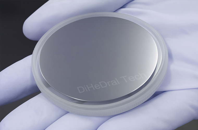
InAs/GaAs epitaxial wafer refers to a heterostructure material system in which indium arsenide (InAs) quantum dots, quantum wells, or thin films are grown on a gallium arsenide (GaAs) single crystal substrate using molecular beam epitaxy (MBE) or metal organic chemical vapor deposition (MOCVD) techniques.
This type of structure typically has strain control and bandgap engineering properties, and is widely used in infrared detectors, high-speed electronic devices, and optical communication fields.
Performance Characteristics
| Properties | Feature Description |
|---|---|
| Bandgap structure | InAs has a narrow bandgap (~0.36 eV), while GaAs has a wider bandgap (~1.42 eV), forming a band step heterojunction |
| High electron mobility | Electron mobility up to 30000 cm ²/V · s, suitable for high-speed devices |
| Strain control structure | There is lattice mismatch (about 7%) in the growth of InAs on GaAs, which can form self-assembled quantum dots (QDs) |
| Adjustable emission wavelength | By adjusting the thickness, strain, and spacing layer of InAs, the emission wavelength can be controlled to 1.0-1.6 μ m (communication band) |
| Good thermal stability | GaAs substrate provides good thermal stability and is suitable for constructing multi-layer structural devices |
Typical applications
Mid infrared photodetectors (MIR photodetectors)
InAs/GaAs quantum well infrared detector (QWIP)
Used for gas detection, night vision imaging, aerospace detection, etc
Optical communication laser
InAs/GaAs self-assembled quantum dot laser (QD Laser)
The working wavelength covers 1.3-1.55 μ m and is a key component of fiber optic communication
High speed electronic devices
Used for high-speed field-effect transistors (FETs) such as HEMTs (high electron mobility transistors) and THz detectors
Single photon source, quantum computing
InAs/GaAs quantum dot structure is an important platform for realizing quantum dot single photon emitters
Applications
This type of structure typically has strain control and bandgap engineering properties, and is widely used in infrared detectors, high-speed electronic devices, and optical communication fields.
Features
Heterogeneous integration has strong compatibility: it can be combined with various III-V materials such as GaAs, InP, AlGaAs to form composite structures
Significant quantum size effect: suitable for quantum dot devices and precision laser applications
High efficiency and low threshold laser emission: InAs QD lasers have higher energy efficiency than traditional InGaAs QW devices
Compatible with mature MOCVD/MBE processes: stable process, high repeatability, and capable of large-scale epitaxial preparation